page 3/64 HiLoNC V2 APPLICATION NOTE Note d’étude / Technical document : URD1– OTL 5665.3– 003 / 72238 Edition 01 Document Sagemcom Reproduction et divulgation interdites Sagemcom document.
page 4/64 SOMMAIRE / CONTENTS 1. OVERVIEW...................................................................................................................................................................7 1.1 OBJECT OF THE DOCUMENT.........................................................................................................................7 1.2 REFERENCE DOCUMENTS.............................................................................................................................7 1.
page 5/64 RECOMMENDED I/OS AND COMPONENTS ON THE FINAL PRODUCT .........................................................42 ESD & EMC RECOMMENDATIONS .......................................................................................................................42 6.1 HILONC V2 ALONE...........................................................................................................................................42 6.2 HANDLING THE MODULE ........................................................
page 6/64 FIGURES LIST Figure 1: Block diagram of HiLoNC module ...........................................................................................................................8 Figure 2: Postage stamp sized HiLoNC V2 51 pads out front side ........................................................................................11 Figure 3: Postage stamp sized HiLoNC V2 51 pads out back side.........................................................................................
page 7/64 1. OVERVIEW 1.1 OBJECT OF THE DOCUMENT The aim of this document is to describe some examples of hardware solutions for developing products around the SAGEMCOM HiLoNC V2 GPRS Module. Most parts of these solutions are not mandatory. Use them as suggestions of what should be done to have a working product and what should be avoided thanks to our experiences.
page 8/64 2. BLOCK DIAGRAM Figure 1: Block diagram of HiLoNC module Note d’étude / Technical document : URD1– OTL 5665.3– 003 / 72238 Edition 01 Document Sagemcom Reproduction et divulgation interdites Sagemcom document.
page 9/64 3. HILONC FAMILY LEGACY 3.
E45 E46 E47 E48 E49 E50 E51 /SIM_RST /SIM_DATA VSIM VBATT GND /HSET_OUT_P /HSET_OUT_N SIM SIM SIM POWER POWER AUDIO AUDIO /SIM_RST /SIM_DATA VSIM VBATT GND /HSET_OUT_P /HSET_OUT_N SIM SIM SIM POWER POWER AUDIO AUDIO page 10/64 P2P Compliant P2P Compliant P2P Compliant P2P Compliant P2P Compliant P2P Compliant P2P Compliant As seen in the table above, the two modules are almost pad to pad (P2P) compliant for the main important signals, however the new HiLoNC V2 M2M module introduce some new interesting
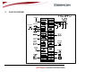
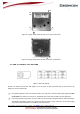
page 11/64 26 40 14 51 1 Figure 2: Postage stamp sized HiLoNC V2 51 pads out front side 1 Figure 3: Postage stamp sized HiLoNC V2 51 pads out back side 4.1 HOW TO CONNECT TO A SIM CARD Figure 4: SIM Card signals HiLoNC V2 module provides the SIM signals on the 51 pads. A SIM card holder with 6 pads needs to be adopted to use the SIM function.
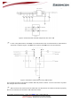
page 12/64 Figure 5: Protections: EMC and ESD components close to the SIM In case of long SIM bus lines over 10cm, it is recommended to also use serial resistors to avoid electrical overshoots on SIM bus signals. Use 56Ω for the clock line and 10Ω for the reset and data lines. Figure 6: Protections: Serial resistors for long SIM bus lines. The schematic here above includes the hardware SIM card presence detector. It can be connected to any GPIO and managed with an AT command.
page 13/64 4.2 HOW TO CONNECT THE AUDIOS? The HiLoNC V2 module features one input audio path and one output audio path. The input path is single-end while the output path is differential. In this following chapter examples of design will be given including protections against EMC and ESD and some notes about the routing rules to follow to avoid the TDMA noise sometimes present in this sensitive area of design.
page 14/64 4.2.1.1 Notes for microphone Pay attention to the microphone device, it must not be sensitive to RF disturbances. If you need to have deported microphone out of the board with long wires, you should pay attention to the EMC and ESD effect. It is also the case when your design is ESD sensitive. In those cases, add the following protections to improve your design.
page 15/64 Figure 10: Example of D class TPA2010D1 1Watt audio amplifier connections. 4.2.2 Recommended characteristics for the microphone and speaker 4.2.2.1 Recommended characteristics for the microphone Item to be inspected Sensitivity Acceptance criterion - 40 dB SPL +/-3 dB (0 dB = 1 V/Pa @ 1kHz) Frequency response Limits (relatives values) Freq. (Hz) Lower limit 100 -1 200 -1 300 -1 1000 0 2000 -1 3000 -1.5 3400 -2 4000 -2 Upper limit 1 1 1 0 1 1.
page 16/64 4.2.3 DTMF OVER GSM NETWORK Former systems used to transmits data through DTMF modulation on RTC telephone lines. Audio DTMF tones are not guarantee over GSM network This is due to the nature of the GSM Voice CODEC - it is specifically designed for the human voice and does not faithfully transmit DTMF. When you press the buttons on your GSM handset during a call, this goes in the Signalling channel - it does not generate in-band DTMF; the actual DTMF tones are generated in the network.
page 17/64 4.4 NETWORK LED The HiLoNC V2 module can manage a network LED. The LED can be connected either to one of the available GPIO or to a PWM (but not the one dedicated to the buzzer). The transistors can be found a in a single package referenced as UMDXX or PUMDXX Family. Value of resistor R depends on characteristic of chosen LED; it is used to limit the current through the diode. Use the AT command to set the GPIO or PWM used to control the LED.
page 18/64 4.5.2 Ripples and drops Current burst at 1.8A 33dBm GSM TX Lev 5 Ripple VBAT drop 3.2V Min Figure 14: GSM/GPRS Burst Current rush and VBAT drops and ripples The minimum voltage during the drop of VBAT must be 3.2V at 33dBm at pads 30 and 31 for the full range of the required functioning temperature. To reach this aim, adapt the VBAT tracks width to minimize the loss: the shorter and thicker is the track; the lower is the serial impedance.
page 19/64 Figure 15: Example of power supply based on a DC/DC step down converter 4.6.2 Simple high current low dropout voltage regulator. If the whole power consumption is not an issue, this example of a simple voltage regulator preceded by an AC/DC to 5V converter, can be use to power the module. The voltage output is given by: VOUT = 1.235V × [1 + (R1 / R2)] To have 3.7V out R1=560K & R2=271.8K (270K+1.
page 20/64 4.6.3 Simple 4V boost converter. Simple boost converter with Linear LT1913 (see LT1316 evaluation kit document). The input can be preceded by an AC/DC converter to get the 5V. PGOOD signal can be checked before the ignition of the module. Figure 17: Example with Linear LT1913 4.7 UART The HiLoNC V2 module features a V24 interface to communicate with the host through AT commands or for easy firmware upgrading purpose.
page 21/64 Consult the AT command Specification document for the use of the UART signals. Unused signals can be left not connected. 4.7.2 Complete V24 – connection HiLoNC V2 - host A V24 interface is provided on the 51 pads of the HiLoNC V2 module with the following signals: RTS/CTS, RXD/TXD, DSR, DTR, DCD, RI. The use of this complete V24 connection is recommended as soon as your application needs to exchange data (over GPRS or CSD).
page 22/64 Avoid supplying the UART before the HiLoNC V2 module is ON, this could result in bad power up sequence. 4.7.3 Complete V24 interface with PC It supports speeds up to 115.2 Kbps and may be used in auto bauding mode. To use the V24 interface, some adaptation components are necessary to convert the +2.8V signals from the HiLoNC V2 to +/- 5V signals compatible with a PC.
page 23/64 Figure 21: Example of a connection to a data cable with a MAX3238E 4.7.4 Partial V24 (RX-TX-RTS-CTS) – connection HiLoNC V2 - host When using only RX/TX/RTS/CTS instead of the complete V24 link, the following schematic could be used. HiLoNC V2 Module 39 40 33 34 35 36 38 37 DTE Device RXD CTS DSR DCD RI DTR TXD RTS TXD CTS DSR DCD RI DTR RXD RTS 2.8V signals 2.
page 24/64 DCD and RI can stay not connected and floating when not used. RI signal is a stand alone signal that can be used with anyone of the following configuration. Consult the AT command specification for more information about this signal and its use.
page 25/64 As DSR is active (low electrical level) once the HiLoNC V2 is switched on, DTR is also active (low electrical level), therefore AT command AT+Ksleep can switch between the two sleep modes available for the HiLoNC V2. DTR input signal is internally pull upped to VGPIO with a 100KΩ, this result in 28µA of extra consumption.
page 26/64 4.9 GPIO There are Three GPIOs available on HiloNC V2. All GPIOs have internal pull-up resistors. GPIOs can directly be controlled with dedicated AT commands.
page 27/64 VBAT R RF_TX HiLoNC V2 Figure 27: RF_TX burst indicator 4.13 BACKUP BATTERY 4.13.1 Backup battery function feature 4.13.1.1 With backup battery A backup battery can be connected to the module in order to supply internal RTC (Real Time Clock) when the main power supply is removed. Thus, when the main power supply is removed, the RTC is still supplied and the module keeps the time register running. With external backup battery: • If VBAT < 3V, internal RTC is supplied by VBACKUP.
page 28/64 Pad Name VBACKUP Min Max 1000µA 4.13.3 Charge by internal HiLoNC V2 charging function The charging function is available on the HiLoNC V2 without any additional external power supply (the charging power supply is provided by the HiLoNC V2). Charge of the back-up battery occurs only when main power supply VBAT is provided.
page 29/64 4.13.4.2 Capacitor battery These kinds of backup battery have not the drawbacks of the Lithium Ion rechargeable battery. As there are only capacitors: • The maximum discharge current is generally bigger, • There is no problem of over-discharge: the capacitor is able to recover its full charge even if its voltage has previously fallen to 0V. • There is no need to regulate the charging current.
page 30/64 4.14 START THE MODULE PROPERLY AND AVOID POWER UP ISSUES. This chapter gives advices on how to make a proper start of the HiLoNC V2 module and sums up the side effects of a non compliant power up sequence or a non compliant hardware connection between the HiLoNC V2 and the host CPU. 4.14.1 Power domains Each HiLoNC V2 pad is linked to a specific internal power domain as the following: • VANA is typically 2.85V and is a general purpose analogue dedicated voltage. • VBAT is typically 3.2V to 4.
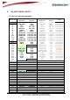
page 31/64 HiLoNC Signal Name Function Power domain Pads E26 /GPIO3 GPIO 2.8V E27 GND RF 0V E28 /ANTENNA RF 3.7V E29 GND RF 0V E30 VBATT POWER 3.7V E31 VBATT POWER 3.7V E32 /UART0_TXD UART 0 2.85V E33 /UART1_DSR UART 1 2.8V E34 /UART1_DCD UART 1 2.8V E35 /UART1_RI UART 1 2.8V E36 /UART1_DTR UART 1 2.8V E37 /UART1_RTS UART 1 2.85V E38 /UART1_RX UART 1 2.85V E39 /UART1_TX UART 1 2.85V E40 /UART1_CTS UART 1 2.85V E41 /POK_IN POWER ON 3.0V E42 /PWM2 PWM 2.85V E43 /PWM1 PWM 2.85V E44 /SIM_CLK SIM 1.8V or 2.
page 32/64 To avoid any power up issue, here are the rules: Avoid any over voltage on the buses lines connected to the module. When the module is off, do not apply any voltage on lines connected to the module. The over voltage can be avoided by using the same power domain voltage. Avoid 5V or 3.3V systems straight connection to 2.8V HiLoNC V2 lines. Use level adaptors when the power domain requires it.
page 33/64 If a straight connection is used between the HiLoNC V2 and the DTE UART it is necessary to isolate host and HiLoNC V2 module in order to avoid generating current re-injection through when HiLoNC V2 is switchedoff.
page 34/64 • To avoid any current re-injection on VPERM (3.0V) The POK_IN signal is internally pulled up and can be connected to an open drain transistor. • To avoid any current re-injection on VRTC (3.0V) The VBACKUP signal has to be only connected to a DC coin 3V battery or a capacitor of 10µF. • To avoid any current re-injection on VSIM (1.8V or 2.9V) Use only VSIM pads to supply the sim card or sim chip. • To avoid any current re-injection on VBAT (3.2V to 4.
page 35/64 Module is OFF Module is ON 2000ms POK_IN VGPIO Software Loading spike Module is ready to receive AT commands CTS Typ 5 seconds Max 7 seconds Figure 35: Power ON sequence Note d’étude / Technical document : URD1– OTL 5665.3– 003 / 72238 Edition 01 Document Sagemcom Reproduction et divulgation interdites Sagemcom document.
page 36/64 4.15 UART SIGNALS AT POWER ON The UART signals are low level active therefore these signals rise up when the module starts. During around 70ms (see figure below), those signals present a transient spike. Those spikes behaviour at start up are normal, however pay attention to them when a CTS low level detection is used do send AT commands. Only DSR and CTS signals get low after the end of the start up procedure.
page 37/64 4.16 POWER ON AND SLEEP DIAGRAMS Those 2 diagrams show the behaviours of the module and the DTE during the power on and then in the sleep modes. DTE is in idle mode U.A.R.T. closed ? VBAT≥3.2 Volts min stable? POK_IN LOW for 2s AND Reset High? VGPIO rise to 2.8V CTS is Low and /or KSUP notified if KSREP activated Module is ready to receive and send AT Figure 37: Diagram for the power on Note d’étude / Technical document : URD1– OTL 5665.
page 38/64 Module is ready to receive and send AT Sleep mode request Ksleep = 1 OR ( Ksleep = 0 AND DTR = High) Delay to enter the sleep mode VGPIO remains at 2.8V CTS is High DTE could also be in sleep mode The wakes up periods are set by the network DRX or the OS Module is in sleep mode Wake up incoming event such as: • Network event. • Alarm interruption. • DTR interruption. • RTS interruption.
page 39/64 4.17 MODULE RESET To reset the module, a low level pulse must be sent on RESET pad during 10 ms. This action will immediately restart the HiLoNC V2 module. It is therefore useless to perform a new ignition sequence (POK_IN) after. SAGEMCOM recommends using this feature in case of emergency, freeze of module or abnormal longer time to respond to AT Commands, this signal is the only way to get the control back over the HiLoNC V2 module.
page 40/64 Figure 40: Power supply command by a GPIO This kind of schematic could also be used to save few micro amperes in case of need. As the module has a drain current of up to 56µA, this kind of function could lower it to the current through R4. These, are the behaviours of the VGPIO and the CTS signal during the power off sequence.
page 41/64 Figure 42: Power consumption at DRX9 (with RS-NGMO2 power supply) When the HiLoNC V2 module leaves the sleep mode thanks to the network incoming signal or by action of the user the power consumption will step from the <1.7mA to 15mA and then to 25mA in around 2 seconds. The behaviour of the system at wake-up: • • System resumes from clock 32 MHz, the power consumption rises to around 15mA. System resumes the hardware blocks, the power consumption rises to around 25mA.
page 42/64 5. RECOMMENDED I/OS AND COMPONENTS ON THE FINAL PRODUCT The design of the customer’s board (on which the module is soldered) must provide an access to following signals when the final product will be completely integrated. To upgrade the module software, SAGEMCOM recommends providing a direct access to the module serial link through an external connector or any mechanism allowing the upgrade of the module without opening the whole product.
page 43/64 6.5 Recommendations to avoid ESD issues Insure good ground connections of the HiLoNC V2 module to the customer’s board. Flex (if any) shall be shielded and FPC connectors shall be correctly grounded at each extremity. Put capacitor 100nF on battery, or better put varistor or ESD diode in parallel on battery and charger wires (if any) and on all power wires connected to the module.
page 44/64 For antenna detection presence circuit refer to the dedicated document: URD1 OTL 5365.1 065 71466 ed 01 - Hilo-HiLoNC Antenna Detection Figure 44: Antenna detection circuit 7.2 GROUND LINK AREA SAGEMCOM emphasizes the fact that a good ground GND contact is needed between the module and the customer’s board to have the best radio performances (spurious, sensitivity…). All HiLoNC V2 GND pads must be connected to the GND of the customer’s board.
page 45/64 7.3 LAYOUT Isolate RF line and antenna from others bus or signals No signals on 50 ohms area and if that is not possible, add ground shielding using different layers. Do not add any ground layer under the antenna contact area.
page 46/64 7.4 MECHANICAL SURROUNDING Do not apply mechanical pressure over the HiLoNC V2 shield, this could damage the mechanical structure of the shield and lead to internal short-circuits or other undesirable issues. Avoid any metallic part around the antenna area Keep FPCs and battery contact (if any) far from antenna area. FPC's (if any) have to be shielded 7.
page 47/64 As audio input and output are strongly linked: Place the microphone and the speaker as far as possible from one another. 8.2 ELECTRONICS AND LAYOUT Avoid Distortion & Burst noise Audio signals must be symmetric (same components on each path). Differential signals must be routed parallel. Audio layer must be surrounded by 2 ground layers. The link from one component to the ground must be as short as possible. If possible separate the PCB of the microphone and the one of the speaker.
page 48/64 9.1.3 Clocks Clock signals must be shielded between two grounds layer and bordered with ground vias. 9.1.4 Data bus and other signals Data bus and commands have to be routed on the same layer; none of the lines of the bus shall be parallel to other lines Lines crossing shall be perpendicular Suitable other signals track width, thickness. Data bus must be protected by upper and lower ground plans 9.1.5 Radio Provide a 50 Ohm micro strip line for antenna connection 9.1.
page 49/64 9.2 EXAMPLE OF LAYOUT FOR CUSTOMER’S BOARD The following figure shows an example of layer allocation for a 6 layers circuit (for reference only): Depending on the customer’s design the layout could also be done using 4 layers. Layer 1: Components (HiloNC) Layer 2: Bus Layer 3: Power supply Layer 4: Complete GND layer Layer 5: Audio, clocks, sensitive signals Layer 6: GND,test points Figure 49: layer allocation for a 6 layers circuit 10.
page 50/64 Figure 50: Factory Tape dimensions Note d’étude / Technical document : URD1– OTL 5665.3– 003 / 72238 Edition 01 Document Sagemcom Reproduction et divulgation interdites Sagemcom document.
page 51/64 10.3 STENCIL Below are given soldering characteristics to report the HiLoNC V2 on the customer’s board. Copper footprint is shown in solid line on the figure below. Stencil footprint is shown in dotted line. Note that the opening and the pads do not strictly recover themselves. Figure 51 : Solder mask design 10.4 SOLDER PASTE SAGEMCOM recommends a stencil thickness of 135 µm. SAGEMCOM recommends use of a “no clean” solder paste.
page 52/64 10.5 PROFILE FOR REFLOW SOLDERING A convection type soldering oven is recommended. Typical usable profile is shown on the next figure.
page 53/64 10.6.1 Nozzles SAGEMCOM recommends using SMT machine with nozzle diameters up to 8 mm in order to always have best prehension of the HiLoNC V2 module. SAGEMCOM recommends using the following two references of nozzles: • For the UNIVERSAL GSM FLEXJET the nozzle 340F Figure 53 : Flexjet nozzle 340F • For the SIEMENS, the nozzle type 417 Figure 54 : Siemens nozzle 417 Note d’étude / Technical document : URD1– OTL 5665.
page 54/64 10.6.2 Fiducials Optical inspection for placement is possible with SMD fiducials placed on the bottom side of the HiLoNC V2. SMD fiducials are not symmetrical in order to help optical inspection to define the right orientation. Figure 55 : Fiducials positions 10.7 UNDERFILL Despite its important reliability, some customer could request for some specific and extreme applications the underfill of onboard components.
page 55/64 Underfill Injection Holes Figure 56 : Underfill injection holes 10.8 SECOND REFLOW SOLDERING Even if SAGEMCOM recommends a single reflow soldering, a second reflow soldering can be conceivable (only if underfill has not been already performed). Positive tests have been performed with HiLoNC V2 on the bottom side. Second reflow soldering is not possible if HiLoNC V2 module has been already under filled. 10.9 HAND SOLDERING Hand soldering is possible.
page 56/64 HiLoNC Electronic board Cube to concentrate the heat Unsoldering hot plate Figure 57 : Laboratory hot plate to unsolder the module 11. Customer must remember to not have components on the HiLoNC V2 opposite side of the customer’s board. LABEL The HiLoNC V2 module is labelled with its own FCC ID(TBD) on the shield side. When the module is installed in customer’s product, the FCC ID label on the module will not be visible.
page 57/64 12. REFERENCE DESIGN: HiLoNC V2 DEVELOPMENT KIT Note d’étude / Technical document : URD1– OTL 5665.3– 003 / 72238 Edition 01 Document Sagemcom Reproduction et divulgation interdites Sagemcom document.
page 58/64 Note d’étude / Technical document : URD1– OTL 5665.3– 003 / 72238 Edition 01 Document Sagemcom Reproduction et divulgation interdites Sagemcom document.
page 59/64 Note d’étude / Technical document : URD1– OTL 5665.3– 003 / 72238 Edition 01 Document Sagemcom Reproduction et divulgation interdites Sagemcom document.
page 60/64 Note d’étude / Technical document : URD1– OTL 5665.3– 003 / 72238 Edition 01 Document Sagemcom Reproduction et divulgation interdites Sagemcom document.
page 61/64 Note d’étude / Technical document : URD1– OTL 5665.3– 003 / 72238 Edition 01 Document Sagemcom Reproduction et divulgation interdites Sagemcom document.
page 62/64 Note d’étude / Technical document : URD1– OTL 5665.3– 003 / 72238 Edition 01 Document Sagemcom Reproduction et divulgation interdites Sagemcom document.
page 63/64 Note d’étude / Technical document : URD1– OTL 5665.3– 003 / 72238 Edition 01 Document Sagemcom Reproduction et divulgation interdites Sagemcom document.
page 64/64 Note d’étude / Technical document : URD1– OTL 5665.3– 003 / 72238 Edition 01 Document Sagemcom Reproduction et divulgation interdites Sagemcom document.