
User's Manual


REV 0.1
Samsung Electro
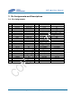
3.2
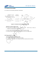
Pin Description
Pin# Signal Name Type
JTAG Interface
33 JTAG_CLK
I
47 JTAG_TDO
O
45 JTAG_TMS
I
49 JTAG_TDI
I
51 JTAG_RST_N
I
31 JTAG_RTCK
O
UART Interface
23 TXD0
O
25 RXD0
I
USB Interface
38 USB_D-
IO
36 USB_D+
IO
UIM Interface
10 UIM_IO
IO
12 UIM_CLK
O
14 UIM_RST_N
O
GPIOs and Miscellaneous
22 PERST# I
20 W_DISABLE#
I
42 LED_WWAN# O
Power Supplies
41 +3.3V I
39 +3.3V I
52 +3.3V I
24 +3.3V I
8 VDD_UIM
O
2 +3.3V
I
Ground
43 GND -
37 GND -
35 GND -
29 GND -
27 GND -
21 GND -
15 GND -
9 GND -
50 GND -
40 GND -
SCF-
V01
Samsung Electro
-Mechanics
Proprietary and Confidential
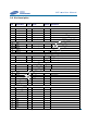
Connection to
IC Pin
Power
Domain
Description
CP_TCK (N.C) JTAG Clock
CP_TDO (N.C) Data Out
CP_TMS (N.C) Mode Selec
t
CP_TDI (N.C) Data In
CP_TRST_N (N.C) JTAG Reset
CP_RTCK (N.C)
JTAG Return Clock
CP_UART0_OUT (N.C) UART0
data out
CP_UART0_IN (N.C) UART0
data in
USB_DMN
Inverted USB transceiver data
USB_DPS Non-
inverted USB transceiver data
UIM_IO
UIM data input-
output
UIM_CLK
UIM clock signal
UIM_RSTN
UIM reset signal
PM Reset Functional Reset
GPIO[01] RF Disable
, Active low signal
GPIO[06]
Status indicator via LED device, Active low signal
3.3V Source
3.3V Source
3.3V Source
3.3V Source
UIM power output
3.3V Source
Ground
Ground
Ground
Ground
Ground
-
Ground
-
Ground
-
Ground
-
Ground
-
Ground
V01
User Manual
Proprietary and Confidential
8/16
t
JTAG Return Clock
data out
data in
Inverted USB transceiver data
inverted USB transceiver data
output
, Active low signal
Status indicator via LED device, Active low signal
UIM power output