COLOR MONITOR SyncMaster SyncMaster SyncMaster SyncMaster SERVICE 330TFT 530TFT 331TFT 531TFT Manual COLOR MONITOR CONTENTS 1. Precautions 2. Reference Information 3. Product Specifications 4. Operating Instructions 5. Disassembly & Reassembly 6. Troubleshooting 7. Exploded View & Parts List 8. Block Diagram SAMSUNG EXIT MENU - + 9. Electrical Parts List 10. PCB Diagrams 11. Wiring Diagram 12.
1 Precautions Follow these safety, servicing and ESD precautions to prevent damage and to protect against potential hazards such as electrical shock. 1-1 Safety Precautions 1-1-1 Warnings 1. For continued safety, do not attempt to modify the circuit board. 2. Disconnect the AC power and DC Power Jack before servicing. 3. (READING SHOULD NOT BE ABOVE 0.5mA) When the chassis is operating, semiconductor heatsinks are potential shock hazards.
1 Precautions 1-2 Servicing Precautions WARNING: An electrolytic capacitor installed with the wrong polarity might explode. Caution: Before servicing units covered by this service manual, read and follow the Safety Precautions section of this manual. Note: If unforeseen circumstances create conflict between the following servicing precautions and any of the safety precautions, always follow the safety precautions. 1-2-1 General Servicing Precautions 1. 2. 3.
2 Reference Information 2-1 List of Abbreviations, Symbols and Acronyms 2-1-1 Abbreviations Abbreviation AUTO_MENB AUTO_SOG BL_EN BRIGHT DAB(7:0) DAG(7:0) DAR(7:0) DBB(7:0) DBG(7:0) DBR(7:0) DDC_SCL DDC_SDA DEN DFSYNCB DHCLK DHS DREFCLK1 DV_BLU DV_FBK DV_GRN DV_RED DVACTIV1B DVCLK DVS DVSYNCB FSD(47:0) HSYNC_PLL INVERT KEY1 KEY2 LED LVDS_DATA LVDS_EN M_HSYNC M_HSYNC1 M_VSYNC M_VSYNC1 OSCOUT Definition AUTO ENABLE (NEG.
2 Reference Information 2-1-2 Symbols Hot Ground Cold Ground ! Provides special safety considerations 2-1-2 Acronyms Acronym Definition Acronym Definition ABL Automatic Brightness Limits H/V Horizontal/Vertical AC Alternating Current HV High Voltage ACL Automatic Contrast Limit I/O Input/Output AFC Automatic Frequency Control IC Integrated Circuit ANSI American National Standards Institute LED Light Emitting Diode CMOS Complementary Metal Oxide Semiconductor MAC Macintosh MOFA
3 Product Specifications 3-1 Specifications Item Description LCD Panel TFT-LCD panel, RGB vertical stripe, normaly white, 15-Inch viewable, 0.297 (H) x 0.297 (V) pixel pitch, 13.3-Inch viewable, 0.264 (H) x 0.264 (V) pixel pitch Scanning Frequency Horizontal : 30 kHz to 61 kHz (Automatic) Vertical : 50 Hz to 75 Hz (Automatic) Display Colors 16.7 Million colors Maximum Resolution Horizontal : 1024 Pixels Vertical : 768 Pixels Input Video Signal Analog, 0.
3 Product Specifications 3-2 Pin Assignments Sync Type 15-Pin Signal Cable Connector Separate Pin No. 1 2 3 4 5 6 7 8 9 10 11 12 13 14 15 Red Green Blue GND GND (DDC Return) GND-R GND-G GND-B No Connection GND-Sync/Self Test GND DDC Data H-Sync V-Sync DDC Clock Sync Type Pin No.
3 Product Specifications 3-3 Timing Chart This section of the service manual describes the timing that the computer industry recognizes as standard for computer-generated video signals. Table 3-1. Timing Chart Mode IBM VESA VGA1/70 Hz 640 x 350 VGA2/70 Hz 720 x 400 VGA3/60 Hz 640 x 480 640/72 Hz 640 x 480 640/75 Hz 640 x 480 800/56 Hz 800 x 600 800/60 Hz 800 x 600 fH (kHz) 31.469 31.469 31.469 37.861 37.500 35.156 37.879 A µsec 31.778 31.777 31.778 26.413 26.667 28.444 26.
3 Product Specifications Table 3-1. Timing Chart Continued Mode MAC. VESA 800/72 Hz 800 x 600 800/75 Hz 800 x 600 1024/60 Hz 1024 x 768 1024/70 Hz 1024 x 768 1024/75 Hz 1024 x 768 640/67 Hz 60 x 480 832/75 Hz 832 x 624 fH (kHz) 48.077 46.875 48.363 56.476 60.023 35.000 49.726 A µsec 20.800 21.333 20.677 17.707 16.660 28.571 20.110 B µsec 2.400 1.616 2.092 1.813 1.219 2.116 1.117 C µsec 1.280 3.232 2.462 1.920 2.235 3.175 3.910 D µsec 16.000 16.162 15.754 13.
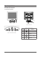
4 Operating Instructions 4-1 Control and Connectors 4-1-1 SyncMaster 331TFT/531TFT SAMSUNG EXIT MENU - + 1 Power Port DC 12V - + 2 Signal Cable Figure 4-2. Rear View G EXIT MENU - Table 4-1. Front Panel Controls + Location 3 4 5 Symbol Description 1 Power Button 2 Power Indicator Figure 4-1.
4 Operating Instructions 4-1-2 SyncMaster 330TFT/530TFT SAMSUNG EXIT 2 MENU - + Audio in port 1 MIC AUDIO OUT IN Headphone jack External microphone jack Microphone out port Power port Figure 4-4. Rear View SAMSUNG EXIT MENU - 3 Table 4-2. Front Panel Controls 4 + Location 5 ON/OFF VOLUME MIN 6 TREBLE BASS MAX MIN MAX 7 MIN MAX 8 MIC ON Symbol Description 1 Power Button OFF 2 Power Indicator 9 3 EXIT Menu Button 4 MENU Exit Button 10 11 5 Figure 4-3.
4 Operating Instructions 4-2 Microprocessor Controls and Functions This monitor has no Òservice onlyÓ micom controls. Should there be a problem with the microprocessor, replace the entire circuit board. There are, however, user accessible adjustment features that are described below. This monitor has factory preset display settings for each of the signals listed in the standard display modes Timing Chart (see pages 3-3 and 3-4).
4 Operating Instructions 4-3 Audio Controls Your LCD monitor provides four audio control buttons located on the front of the stand. 4-3-1 Audio Adjustments To access the on/off, volume, bass and treble functions push the appropriate blue control button until it pops out then turn it to the right or left to adjust the function.
5 Disassembly and Reassembly This section of the service manual describes the disassembly and reassembly procedures for the SyncMaster 33*TFT/53*TFT monitors. WARNING: This monitor contains electrostatically sensitive devices. Use caution when handling these components. 5-1 Disassembly Cautions:1. Disconnect the monitor from the power source before disassembly. 2. Follow these directions carefully; never use metal instruments to pry apart the cabinet. 5-1-1 Removing the Stand 5.
5 Disassembly and Reassembly 6. Remove 4 screws on the Rear Panel Bracket. (15Ó : 6 screws) Figure 5-5 7. Remove the Bracket Assembly from the Front Cover. Figure 5-7 14. Remove 2 screws between Rear Bracket and Inverter PCB. 8. Remove 1 screw on the Power PCB. 15. Remove the Interface wire on the Rear Side of Panel. 9. Remove Function PCB from locking area of Function Knob. 5-1-3 Stand Disassembly 1. Stand the stand assembly with the base close to you. Figure 5-6 10.
5 Disassembly and Reassembly 2. Make a little gap between stand assembly and Rear Cover with a ÔÐÕ screw driver. And pry Rear Cover off stand assembly with the finger. 5. Remove the screw and washer on the base of the stand. Figure 5-11 Figure 5-9 6. Remove the Stand Base and Stand Top. 3. Remove the 10 screws from the stand assembly. Figure 5-10 4. Remvoe the hinge, neck front, PCB, signal cable.
5 Disassembly and Reassembly 5-2 Replacement Order of Lamp Assemblies (13.3”) 1. Disconnect lamp leadconnector from the inverter. * Replacement of lamp assemblies should be done at the power off state and recommended clean bench condition. 2. Remove a screw which is used to hold a lamp assembly on. 3. Replace lamp assemblies. 4. Assemble new lamp assembly according to the counter order.
5 Disassembly and Reassembly 5-3 Replacement Order of Lamp Assemblies (15”) 1. Disconnect lamp leadconnectors from the inverter. (2EA) * Replacement of lamp assemblies should be done at the power off state and recommended clean bench condition. 2. Remove 2 screws which are used to hold the lamp assemblies on. 3. Replace 2 lamp assemblies. 4. Assemble new lamp assemblies according to the counter order.
5 Disassembly and Reassembly 5-4 Reassembly Reassembly procedures are in the reverse order of Disassembly procedures.
6 Troubleshooting Notes: 1. Before troubleshooting, setup the PC’s display as below. • Resolution: 1024 x 768 • H-frequency: 48 kHz • V-frequency: 60 Hz 2. If no picture appears, make sure the power cord is correctly connected. 3. Check the following circuits.
6 Troubleshooting 6-2 No Video Power indicator is green Does the clock pulse appear at output of FT110, FT111, FT112? No 7 Does the H-sync pulse appear at Pin 94 of IC101? No 8 9 Does the pulse appear at Pin 10 of IC105 or Pin 1 of IC104? No Yes Yes Replace IC106. Yes Replace IC105 (seperate sync) or IC104 (SOG). Replace IC101. 18 19 Does the sync pulses appear at Pins 13 and 14 of IC110? No 20 1 Does the sync pulses appear at Pins 2 and 3 of IC110? No Check IC401 and IC101.
6 Troubleshooting WAVEFORMS 1 IC110 #3 CH1 RMS = 3.6 V 5 IC310 #26 CH1 RMS = 2.12 V 2 IC310 #22 CH1 RMS = 3.1 V 6 CN301 #5~20 CH1 RMS = 2.3 V 7 IC101 #94 4 IC310 #25 CH1 RMS = 2.8 V 8 IC105 #10 CH1 RMS = 3.5 V CH1 RMS = 3.1 V 10 IC301 #2 11 IC301 #3 12 IC301 #54 CH1 RMS = 4.56 V CH1 RMS = 2.3 V CH1 RMS = 3.25 V CH1 RMS = 2.35 V 13 IC301, #55 14 IC301 #56 18 IC110 #13 19 IC110 #14 CH1 RMS = 200 mV CH1 RMS = 50 mV CH1 RMS = 1.24 V CH1 RMS = 400 mV 9 IC104, #1 CH1 RMS = 1.
6 Troubleshooting 6-3 No Video of Alternate Vertical Line One or more even or odd vertical lines do not display. 6 Does the waveform appear at Pin 20 of CN301? No WAVEFORMS Replace IC311 or check its related circuit. 6 CN301 #5~20 Yes Replace LCD panel. CH1 RMS = 1.18 V 6-4 No OSD WAVEFORMS There is video but no OSD. 15 While pushing a front control button does any pulse appear at Pin 12 of IC307? 15 IC307 #12 No 16 Do sync signals appear at Pins 5 and 10 of IC307? 17 No CH1 RMS = 2.
6 Troubleshooting 6-6 No Sound (SyncMaster 330TFT/530TFT) Does the DC 5 V appear at Pin 5 of CN806, Pin 4 of IC803? No Check IC804, IC803, VR841 and related circuit. No Check Pins 1 and 2 of CN806 and related circuits. Yes Does the sound input signal appear at Pins 6 and 11 of IC803? Yes Do the sound signals appear at Pins 3 and 14 of IC803? No Check IC803 and related circuits. Yes Does the DC 2.5 V bias appear at Pin 16 of IC503? No Check CN813, ZD803, R821, R822, C815 on the Audio PCB.
6 Troubleshooting 6-7 Microphones Don’t Work (SyncMaster 330TFT/530TFT) Does the PC’s sound program operate well? No Check the PC’s sound program and compatibility. No Connect the cable between the PC and monitor. No Check the connection between CN805 on the Audio PCB and the Internal Microphone. Yes Is the connection between the PC and monitor secure? Yes Is the Internal Microphone connector attached? Yes Does the Internal Microphone work? No Check Q802 and related circuits.
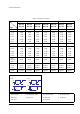
9 Electrical Parts List 9-1 Main PCB Parts Loc. No. BD101 BD102 BD103 BD104 BD105 C100 C101 C102 C103 C104 C105 C106 C107 C108 C109 C110 C111 C112 C113 C114 C115 C116 C117 C118 C119 C120 C121 C122 C123 C124 C125 C126 C127 C128 C129 C130 C131 C132 C133 C134 C135 C136 C137 C138 C139 Code No.
9 Electrical Parts List Loc. No. C140 C141 C142 C143 C144 C145 C146 C147 C148 C149 C150 C151 C152 C153 C154 C155 C156 C157 C158 C159 C160 C161 C163 C165 C166 C167 C168 C169 C170 C172 C173 C174 C175 C176 C177 C180 C181 C182 C183 C184 C185 C186 C187 C188 C189 C190 C195 9-2 Code No.
9 Electrical Parts List Loc. No. C196 C201 C202 C203 C204 C301 C302 C303 C304 C305 C306 C307 C308 C309 C310 C311 C312 C313 C314 C315 C316 C317 C318 C319 C320 C321 C322 C323 C324 C325 C326 C327 C328 C329 C330 C331 C332 C333 C334 C335 C336 C337 C338 C339 C340 C341 C342 Code No.
9 Electrical Parts List Loc. No. C343 C344 C345 C346 C347 C348 C349 C350 C351 C352 C353 C354 C355 C356 C357 C358 C359 C360 C361 C362 C363 C364 C365 C366 C367 C368 C369 C370 C371 C372 C373 C374 C377 C378 C379 C380 C381 C382 C383 C384 C385 C386 C387 C388 C389 C390 C391 9-4 Code No.
9 Electrical Parts List Loc. No. C392 C393 C394 C395 C396 C397 C398 C401 C402 C403 C404 C405 C406 C407 C408 C409 C410 C411 C412 C413 C414 C415 C416 C417 C418 C419 CFT302 CFT317 CFT318 CFT319 CIS CL101 CL102 CN101 CN102 CN103 CN103_PANEL CN301 CN301_PANEL CN401 CN401_CN861 D101 D102 D103 D104 Code No.
9 Electrical Parts List Loc. No. D105 D106 D109 D110 D113 D114 D401 D402 D403 D404 F101 FT101 FT102 FT103 FT120 FT122 FT301 FT306 FT307 FT308 FT309 FT310 FT311 FT312 FT313 FT314 FT315 FT316 FT320 FT321 FT322 FT323 FT324 FT325 FT326 FT327 FT328 FT329 FT330 FT331 FT332 FT333 FT334 FT335 FT390 FT404 IC101 9-6 Code No.
9 Electrical Parts List Loc. No. IC102 IC103 IC104 IC105 IC106 IC107 IC108 IC109 IC110 IC115 IC301 IC302 IC303 IC304 IC305 IC306 IC307 IC308 IC309 IC310 IC311 IC401 IC401_SOCK IC402 IC403 IC404 IC405 IC406 IC803 IC804 L102 L151 L152 L153 L160 L170 L171 L172 L301 L302 L303 L403 L406 L407 Q101 Q301 Q302 Code No.
9 Electrical Parts List Loc. No. Q401 R101 R102 R103 R104 R105 R106 R107 R110 R115 R116 R117 R118 R124 R125 R127 R128 R129 R130 R131 R132 R134 R135 R137 R138 R140 R190 R191 R192 R193 R194 R301 R302 R303 R305 R306 R307 R308 R309 R310 R311 R312 R316 R317 R401 R402 R403 9-8 Code No.
9 Electrical Parts List Loc. No. R404 R405 R406 R407 R408 R409 R410 R411 R412 R413 R415 R416 R417 R418 R419 R420 R421 R422 R423 R424 R425 R426 R427 R429 R431 R432 R433 R436 R437 R438 R439 R440 R441 R442 R443 R444 R445 R447 R448 R449 R450 R451 R452 R455 R456 R457 R458 Code No.
9 Electrical Parts List Loc. No. R459 R460 R461 R462 R463 R464 R465 RA101 RA102 RA103 RA104 RA105 RA106 RA107 RA108 RA109 RA110 RA111 RA112 RA301 RA302 RA303 RA304 RA305 RL101 SW301 VR843 X301 X302 X401 ZD101 ZD102 ZD103 ZD104 ZD105 ZD401 9-10 Code No.
9 Electrical Parts List 9-2 Sub PCB Parts Loc. No. BD801 BD802 BD803 C801 C802 C803 C804 C810 C811 C812 C813 C814 C815 C816 C820 C841 C842 C843 C844 C845 C846 C847 C848 C849 C850 CN801 CN803 CN804 CN805 CN806 CN806_CN841 CN808 CN809 CN810 CN811 CN812 CN813 CN814 CN815 CN816 CN841 CN861 CN862 CN862_CN881 CN881 CN882 D801 Code No.
9 Electrical Parts List Loc. No. D802 IC803 IC804 L801 OP881 Q802 R809 R810 R811 R812 R813 R814 R815 R816 R817 R818 R819 R820 R821 R822 R841 R842 R843 R844 R845 R846 R861 R862 R863 R864 R865 R866 R867 R868 R869 R881 R882 SW841 SW861 SW862 SW863 SW864 SW865 SW866 SW881 VR841 VR842 9-12 Code No.
9 Electrical Parts List Loc. No. VR843 ZD801 ZD802 ZD803 ZD861 ZD862 Code No. 2101-001041 0403-000003 0403-000003 0403-000003 0403-000003 0403-000003 SyncMaster 3*TFT/53*TFT Description VR-ROTARY DIODE-ZENER DIODE-ZENER DIODE-ZENER DIODE-ZENER DIODE-ZENER Specification Remarks 50Kohm,20%,1/20W,TOP UZ8.2BL,8.2V,7.7-8.2V,500mW,DO UZ8.2BL,8.2V,7.7-8.2V,500mW,DO UZ8.2BL,8.2V,7.7-8.2V,500mW,DO UZ8.2BL,8.2V,7.7-8.2V,500mW,DO UZ8.2BL,8.2V,7.7-8.
9 Electrical Parts List Others Loc. No. LCD P/CORD S/CABLE SPEAKER ADAPTOR PROCESS-PBA UNIT B/D ASS’Y CODE 9-14 Code No.
SyncMaster 33*TFT/53*TFT 12V B G R H V 8 8 8 DOT_CLK R G B DOT_CLK TDA8752 H +5 V_S +3.3 V_S VCC +5 V_PLL +5 V_ADL FRAME MEMORY GMFC1 H V MICOM and CONTROL PART 8 8 8 GMZ1 VOLUME TONE CTRL.
8 Block Diagrams Memo 8-2 SyncMaster 33*TFT/53*TFT
10 PCB Diagrams 10-2 Semiconductor Lead Identification PARTS TYPE NO. 431 REF. NO. PARTS TYPE NO. REF. NO.
10 PCB Diagrams PARTS TYPE NO. REF. NO. PARTS 80 48 DS90CF561 TYPE NO. 50 IC310, IC311 100 1 1 REF. NO.
11 Wiring Diagram RIGHT – RIGHT + CN814 1 2 LEFT – LEFT + CN815 1 2 3 4 5 6 7 8 8 7 6 5 4 3 2 1 LEFT_AMP RIGHT_AMP GND MIC_EN 5V 5V LEFT_IN RIGHT_IN CN841 AUDIO FUNC PCB 1 2 3 CN801 LEFT_AMP RIGHT_AMP GND MIC_EN 5V 5V LEFT_IN RIGHT_IN CN806 LIVE GND NEUTRAL 1 2 MIC_GND MIC_SIG GND 12 V CN804 CN808 CN809 MIC_OUT PC_AUDIO CN812 CN813 1 2 CN816 1 2 C-MIC NC GND NC NEUTRAL LIVE 1 2 3 4 5 CN805 EXT_MIC HEADPHONE CN103 MAIN PCB PC_R_IN 1 PC_G_IN 2 PC_B_IN 3 GND 4~9 S_RASTER 10 G
12 Schematic Diagrams 12-1 DAC & IO Part Schematic Diagram 20 1 18 19 7 9 8 Power Line Signal Line 12-1 SyncMaster 33*TFT/53*TFT
12 Schematic Diagrams 1024 x 768 / 85 Hz pin # MODES pin # MODES Table 12-2. IC103 1024 x 768 / 85 Hz 1 2 3 12 GND 5 1 2 3 12 GND 5 Unit: Vrms Unit: Vrms Table 12-3. IC107 MODES pin # Table 12-1. IC102 1024 x 768 / 85 Hz 1 2 3 4 5 12 5 GND 5 GND Unit: Vrms pin # MODES 1024 x 768 / 85 Hz 1 2 3 4 5 12 3.3 GND 3.3 GND Table 12-5. IC109 1 IC110 #3 MODES pin # Table 12-4. IC108 1024 x 768 / 85 Hz 1 2 3 12 GND 5 CH1 RMS = 3.
12 Schematic Diagrams 12-2 ZOOM & FRC Part Schematic Diagram 2 3 5 4 16 15 6 17 12 13 14 10 11 Power Line Signal Line 12-3 SyncMaster 33*TFT/53*TFT
12 Schematic Diagrams Table 12-6. IC309 2 IC310 #22 3 IC310 #23 pin # MODES 1024 x 768 / 85 Hz 1 2 3 4 5 6 7 8 11.96 5.90 4.99 5.8 mV 4.99 4.99 11.95 11.95 CH1 RMS = 3.1 V CH1 RMS = 2.3 V Unit: Vrms 4 IC310 #25 CH1 RMS = 2.8 V 5 IC310 #26 CH1 RMS = 2.12 V 6 CN301 #5~20 CH1 RMS = 1.18 V 10 IC301 #2 11 IC301 #3 12 IC301 #54 CH1 RMS = 2.3 V CH1 RMS = 3.25 V CH1 RMS = 2.
12 Schematic Diagrams 12-3 Micom Part Schematic Diagram Table 12-7. IC401 1024 x 768 / 85 Hz pin # MODES pin # MODES 1024 x 768 / 85 Hz 1 2 3 4 5 6 7 8 9 10 11 12 13 14 15 16 17 18 19 20 21 59.8 mV 5 5 5 4.62 0.457 4.91 5 GND 5.03 5.02 5.02 NC NC 4.94 93.7 mV 3.217 4.97 5.01 63.0 mV 0.476 22 23 24 25 26 27 28 29 30 31 32 33 34 35 36 37 38 39 40 41 42 3.44 GND 4.16 5.01 4.97 4.46 4.43 4.78 4.77 14.07 2.226 2.238 5.03 5.03 4.96 4.96 52.7 mV 4.96 4.87 GND 9.7 mV Unit: Vrms Table 12-8.
12 Schematic Diagrams 12-4 Sub Part Schematic Diagram pin # Table 12-10. IC803 MODES 1024 x 768 / 85 Hz 1 GND 2 GND Signal (+2.5 V Bias) 3 4 5 5 Signal (+2.5 V Bias) 6 Input Signal (+2.5 V Bias) 7 GND 2.5 8 9 2.5 10 2.5 11 Input Signal (+2.5 V Bias) Signal (+2.5 V Bias) 12 13 5 14 Signal (+2.5 V Bias) 15 GND 16 2.
12 Schematic Diagrams Memo 12-7 SyncMaster 33*TFT/53*TFT
Samsung Electronics Co., Ltd. July 1998 Printed in Korea Code No.