LCD-TV Chassis : GJE32ASA-N61A Model : LA32A330J1N** SERVICE TFT-LCD TV Manual Contents 1. Precautions 2. Product specifications 3. Disassembly and Reassembly 4. Troubleshooting 5. Exploded View & Part List 6. Wiring Diagram LA32A330J1N** Refer to the service manual in the GSPN (see the rear cover) for the more information.
Contents 1. Precautions............................................................................................................... 1-1 1-1. Safety Precautions.......................................................................................................... 1-1 1-2. Servicing Precautions...................................................................................................... 1-2 1-3. Electrostatically Sensitive Devices (ESD) Precautions................................................
GSPN (Global Service Partner Network) Area Web Site North America http://service.samsungportal.com Latin America http://latin.samsungportal.com CIS http://cis.samsungportal.com Europe http://europe.samsungportal.com China http://china.samsungportal.com Asia http://asia.samsungportal.com Mideast & Africa http://mea.samsungportal.com This Service Manual is a property of Samsung Electronics Co.,Ltd.
3. Disassembly and Reassembly 3. Disassembly and Reassembly This section of the service manual describes the disassembly and reassembly procedures for the LA32A330J1N** LCD TV. WARNING: This TV contains electrostatically sensitive devices. Use caution when handling these components. 3-1. Disassembly and Reassembly Cautions: 1. Disconnect the LCD TV from the power source before disassembly. 2. Follow these directions carefully; never use metal instruments to pry apart the cabinet.
3. Disassembly and Reassembly Description Picture Description Screws 3. Remove Screw from the stand BRKT. Lift up the stand BRKT.
3. Disassembly and Reassembly Description Picture Description Screws 4. Disconnect a cable from the Main&IP boards. Remove a Cable. 5. Remove the screws of the Main & IP boards. Remove the Main & IP boards.
3. Disassembly and Reassembly Description Picture Description Screws 6. Remove the Screw from Front Assy. Lift up the Panel BRKT. x 10 7. Remove the screws from Panel BRKT. Remove the Panel BRKT. x9 ※ Reassembly procedures are in the reverse order of disassembly procedures.
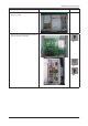
5. Exploded View & Part List 5. Exploded View & Part List T0003 M0215 T0447 M0107 M0254 M0014 T0764 M0115 M0013 M0027 5-1.
5. Exploded View & Part List 5-1-1. LA32A330J1N** Parts List Location No. Code No. T0003 BN96-04969K M0215 Q’ty S.A/S.N.A ASSY COVER P-FRONT;DP,BN96-08138A,HANARO 1 S.A BN07-00572A LCD-PANEL;LTF320AP01 1 S.A M0115 BN61-02947A BRACKET-STAND LINK;JASMINE 32”,SECC,T1.6 1 S.N.A M0014 BN94-02083A ASSY PCB MAIN;CHINA 1 S.A M0013 BN96-08139B ASSY COVER P-REAR;HANARO 32,SO,HIPS,HB,B 1 S.A M0027 BN96-04973B ASSY STAND P-BASE;DP,BN96-04697C,,,,,HAN 1 S.
5. Exploded View & Part List 5-2. LA32A330J1N** Parts List Level Location No. Code No. Description & Specification LA32A330J1NXRD LA32A330J1N,N61A/32S80-GJE,32,LCD-TV,NEW Q’ty SA/SNA 0.1 M0216 BN90-01175U ASSY STAND;HANARO 32,EO 1 S.N.A ..2 M0027 BN96-04697C ASSY STAND P-BASE;HANARO,32,W/W,ABS+PMMA 1 S.A ...3 T0081 6002-001294 SCREW-TAPPING;BH,+,,M4,L16,ZPC(BLK) 4 S.N.A ...3 M0081 6003-001239 SCREW-TAPTITE;FH,+,-,B,M4,L10,ZPC(WHT),S 4 S.N.A ...
5. Exploded View & Part List Level Location No. 0.1 Code No. Description & Specification Q’ty SA/SNA BN91-02535A ASSY LCD-AMLCD;LE32A336J1NX** 1 S.N.A ..2 M0215 BN07-00572A LCD-PANEL;LTF320AP01 1 S.A ...3 M0174 BN44-00235A IP BOARD;32TVINVERTER,HANARO,3.0mA,8.0mA 1 S.A 0.1 M0017 BN91-02573A ASSY CHASSIS;CHINA 1 S.N.A ..2 M0014 BN94-02083A ASSY PCB MAIN;CHINA 1 S.A ...3 T0245 0202-001521 SOLDER-WIRE FLUX;ECO SOLDER RMA98 SUP,-, 0.25 S.N.A ...
5. Exploded View & Part List Level Location No. Code No. Description & Specification Q’ty SA/SNA ....4 D3019 0401-001056 DIODE-SWITCHING;MMBD4148SE,100V,200mA,SO 1 S.A ....4 D3021 0401-001056 DIODE-SWITCHING;MMBD4148SE,100V,200mA,SO 1 S.A ....4 D3022 0401-001056 DIODE-SWITCHING;MMBD4148SE,100V,200mA,SO 1 S.A ....4 D3023 0401-001056 DIODE-SWITCHING;MMBD4148SE,100V,200mA,SO 1 S.A ....4 D3024 0401-001056 DIODE-SWITCHING;MMBD4148SE,100V,200mA,SO 1 S.A ....
5. Exploded View & Part List Level Location No. Code No. Description & Specification Q’ty SA/SNA ....4 D0254 ....4 D2013 0404-001314 DIODE-SCHOTTKY;B260A,60V,2000mA,SMA,TP 1 S.N.A 0407-000123 DIODE-ARRAY;DAN202K,80V,100mA,CA2-3,SOT- 1 S.N.A ....4 ....4 D3071 0407-000123 DIODE-ARRAY;DAN202K,80V,100mA,CA2-3,SOT- 1 S.N.A D3072 0407-000123 DIODE-ARRAY;DAN202K,80V,100mA,CA2-3,SOT- 1 S.N.A ....4 D6 0407-000139 DIODE-ARRAY;-,80V,100mA,CX3,IMD,TP 1 S.A ....
5. Exploded View & Part List Level Location No. Code No. Description & Specification Q’ty SA/SNA ....4 IC112 ....4 IC112 1103-000129 IC-EEPROM;24C02,2Kbit,256x8Bit,SOP,8P,5x 1 S.A 1103-001385 IC-EEPROM;AT24C256,256Kbit,32Kx8,SOP,8P, 1 S.A ....4 IC113 ....4 IC5201 1105-001391 IC-DRAM;EM638325,2MX32BIT,TSOP(II),86P,4 1 S.A 1105-001749 IC-GDDR;K4D261638I,GDDR,128Mbit,4x2Mx16, 1 S.N.A ....4 ....4 DU410 1201-000541 IC-OP AMP;062,SOP,8P,153MIL,DUAL,6V/mV,P 1 S.
5. Exploded View & Part List Level Location No. Code No. Description & Specification Q’ty SA/SNA ....4 R3033 2007-000138 R-CHIP;100ohm,5%,1/16W,TP,1005 1 S.N.A ....4 R3034 2007-000138 R-CHIP;100ohm,5%,1/16W,TP,1005 1 S.N.A ....4 R3037 2007-000138 R-CHIP;100ohm,5%,1/16W,TP,1005 1 S.N.A ....4 R3050 2007-000138 R-CHIP;100ohm,5%,1/16W,TP,1005 1 S.N.A ....4 R3052 2007-000138 R-CHIP;100ohm,5%,1/16W,TP,1005 1 S.N.A ....4 R3058 2007-000138 R-CHIP;100ohm,5%,1/16W,TP,1005 1 S.
5. Exploded View & Part List Level Location No. Code No. Description & Specification Q’ty SA/SNA ....4 R6991_PW 2007-000138 R-CHIP;100ohm,5%,1/16W,TP,1005 1 S.N.A ....4 R88 2007-000138 R-CHIP;100ohm,5%,1/16W,TP,1005 1 S.N.A ....4 R9998 2007-000138 R-CHIP;100ohm,5%,1/16W,TP,1005 1 S.N.A ....4 R1006 2007-000140 R-CHIP;1Kohm,5%,1/16W,TP,1005 1 S.N.A ....4 R1007 2007-000140 R-CHIP;1Kohm,5%,1/16W,TP,1005 1 S.N.A ....4 R1054 2007-000140 R-CHIP;1Kohm,5%,1/16W,TP,1005 1 S.N.
5. Exploded View & Part List Level Location No. Code No. Description & Specification Q’ty SA/SNA ....4 R6068_L 2007-000143 R-CHIP;4.7Kohm,5%,1/16W,TP,1005 1 S.N.A ....4 R6072_PW 2007-000143 R-CHIP;4.7Kohm,5%,1/16W,TP,1005 1 S.N.A ....4 R1009 2007-000148 R-CHIP;10Kohm,5%,1/16W,TP,1005 1 S.N.A ....4 R1061_5V 2007-000148 R-CHIP;10Kohm,5%,1/16W,TP,1005 1 S.N.A ....4 R11 2007-000148 R-CHIP;10Kohm,5%,1/16W,TP,1005 1 S.N.A ....
5. Exploded View & Part List Level Location No. Code No. Description & Specification Q’ty SA/SNA ....4 R3120 2007-000151 R-CHIP;15Kohm,5%,1/16W,TP,1005 1 S.N.A ....4 R3121 2007-000151 R-CHIP;15Kohm,5%,1/16W,TP,1005 1 S.N.A ....4 R3132 2007-000151 R-CHIP;15Kohm,5%,1/16W,TP,1005 1 S.N.A ....4 R3133 2007-000151 R-CHIP;15Kohm,5%,1/16W,TP,1005 1 S.N.A ....4 R3192 2007-000151 R-CHIP;15Kohm,5%,1/16W,TP,1005 1 S.N.A ....4 R3193 2007-000151 R-CHIP;15Kohm,5%,1/16W,TP,1005 1 S.
5. Exploded View & Part List Level Location No. Code No. Description & Specification Q’ty SA/SNA ....4 R1001 2007-000171 R-CHIP;0ohm,5%,1/16W,TP,1005 1 S.N.A ....4 R110 2007-000171 R-CHIP;0ohm,5%,1/16W,TP,1005 1 S.N.A ....4 R111 2007-000171 R-CHIP;0ohm,5%,1/16W,TP,1005 1 S.N.A ....4 R112 2007-000171 R-CHIP;0ohm,5%,1/16W,TP,1005 1 S.N.A ....4 R113 2007-000171 R-CHIP;0ohm,5%,1/16W,TP,1005 1 S.N.A ....4 R114 2007-000171 R-CHIP;0ohm,5%,1/16W,TP,1005 1 S.N.A ....
5. Exploded View & Part List Level Location No. Code No. Description & Specification Q’ty SA/SNA ....4 R3465_CO 2007-000171 R-CHIP;0ohm,5%,1/16W,TP,1005 1 S.N.A ....4 R3466_CO 2007-000171 R-CHIP;0ohm,5%,1/16W,TP,1005 1 S.N.A ....4 R3467_CO 2007-000171 R-CHIP;0ohm,5%,1/16W,TP,1005 1 S.N.A ....4 R3470_CO 2007-000171 R-CHIP;0ohm,5%,1/16W,TP,1005 1 S.N.A ....4 R37_OP 2007-000171 R-CHIP;0ohm,5%,1/16W,TP,1005 1 S.N.A ....
5. Exploded View & Part List Level Location No. Code No. Description & Specification Q’ty SA/SNA ....4 R85 2007-000171 R-CHIP;0ohm,5%,1/16W,TP,1005 1 S.N.A ....4 R87 2007-000171 R-CHIP;0ohm,5%,1/16W,TP,1005 1 S.N.A ....4 R9 2007-000171 R-CHIP;0ohm,5%,1/16W,TP,1005 1 S.N.A ....4 R91 2007-000171 R-CHIP;0ohm,5%,1/16W,TP,1005 1 S.N.A ....4 R94 2007-000171 R-CHIP;0ohm,5%,1/16W,TP,1005 1 S.N.A ....4 R9999 2007-000171 R-CHIP;0ohm,5%,1/16W,TP,1005 1 S.N.A ....
5. Exploded View & Part List Level Location No. Code No. Description & Specification Q’ty SA/SNA ....4 R68 2007-000173 R-CHIP;22ohm,5%,1/16W,TP,1005 1 S.N.A ....4 R69 2007-000173 R-CHIP;22ohm,5%,1/16W,TP,1005 1 S.N.A ....4 R70 2007-000173 R-CHIP;22ohm,5%,1/16W,TP,1005 1 S.N.A ....4 R71 2007-000173 R-CHIP;22ohm,5%,1/16W,TP,1005 1 S.N.A ....4 R72 2007-000173 R-CHIP;22ohm,5%,1/16W,TP,1005 1 S.N.A ....4 R141 2007-000174 R-CHIP;47ohm,5%,1/16W,TP,1005 1 S.N.A ....
5. Exploded View & Part List Level Location No. Code No. Description & Specification Q’ty SA/SNA ....4 R2043 ....4 R1029 2007-000669 R-CHIP;2Kohm,1%,1/10W,TP,1608 1 S.N.A 2007-000708 R-CHIP;3.9Kohm,1%,1/10W,TP,1608 1 S.A ....4 ....4 R168 2007-000708 R-CHIP;3.9Kohm,1%,1/10W,TP,1608 1 S.A R147 2007-000726 R-CHIP;300ohm,1%,1/10W,TP,1608 1 S.A ....4 R148 2007-000726 R-CHIP;300ohm,1%,1/10W,TP,1608 1 S.A ....4 R149 2007-000726 R-CHIP;300ohm,1%,1/10W,TP,1608 1 S.A ....
5. Exploded View & Part List Level Location No. Code No. Description & Specification Q’ty SA/SNA ....4 R142 2007-001125 R-CHIP;68Kohm,1%,1/10W,TP,1608 1 S.A ....4 R134 2007-001153 R-CHIP;750ohm,1%,1/10W,TP,1608 1 S.A ....4 R135 2007-001153 R-CHIP;750ohm,1%,1/10W,TP,1608 1 S.A ....4 R136 2007-001153 R-CHIP;750ohm,1%,1/10W,TP,1608 1 S.A ....4 R176 2007-001153 R-CHIP;750ohm,1%,1/10W,TP,1608 1 S.A ....4 R178 2007-001153 R-CHIP;750ohm,1%,1/10W,TP,1608 1 S.A ....
5. Exploded View & Part List Level Location No. Code No. Description & Specification Q’ty SA/SNA ....4 R108 2007-007136 R-CHIP;4.7Kohm,1%,1/16W,TP,1005 1 S.N.A ....4 R133 2007-007136 R-CHIP;4.7Kohm,1%,1/16W,TP,1005 1 S.N.A ....4 R2076 2007-007136 R-CHIP;4.7Kohm,1%,1/16W,TP,1005 1 S.N.A ....4 R102 2007-007142 R-CHIP;10Kohm,1%,1/16W,TP,1005 1 S.N.A ....4 R1022 2007-007142 R-CHIP;10Kohm,1%,1/16W,TP,1005 1 S.N.A ....4 R1058 2007-007142 R-CHIP;10Kohm,1%,1/16W,TP,1005 1 S.
5. Exploded View & Part List Level Location No. Code No. Description & Specification Q’ty SA/SNA ....4 RA5033 2011-001093 R-NETWORK;100ohm,5%,1/16W,L,CHIP,8P,TP,3 1 S.A ....4 R73 2011-001288 R-NETWORK;18ohm,5%,1/16W,L,CHIP-V,8P,TP, 1 S.N.A ....4 R74 2011-001288 R-NETWORK;18ohm,5%,1/16W,L,CHIP-V,8P,TP, 1 S.N.A ....4 R75 2011-001288 R-NETWORK;18ohm,5%,1/16W,L,CHIP-V,8P,TP, 1 S.N.A ....4 R76 2011-001288 R-NETWORK;18ohm,5%,1/16W,L,CHIP-V,8P,TP, 1 S.N.A ....
5. Exploded View & Part List Level Location No. Code No. Description & Specification Q’ty ....4 C5092 ....4 C3034 ....4 ....4 2203-000489 C-CER,CHIP;2.2nF,10%,50V,X7R,1005 1 S.A 2203-000627 C-CER,CHIP;0.022nF,5%,50V,C0G,1005 1 S.N.A C3035 2203-000627 C-CER,CHIP;0.022nF,5%,50V,C0G,1005 1 S.N.A C5042 2203-000627 C-CER,CHIP;0.022nF,5%,50V,C0G,1005 1 S.N.A ....4 C5043 2203-000627 C-CER,CHIP;0.022nF,5%,50V,C0G,1005 1 S.N.A ....4 C58 2203-000627 C-CER,CHIP;0.
5. Exploded View & Part List Level Location No. Code No. Description & Specification Q’ty SA/SNA ....4 C5037 2203-002793 C-CER,CHIP;1000nF,+80-20%,25V,Y5V,2012 1 S.N.A ....4 C5202 2203-002793 C-CER,CHIP;1000nF,+80-20%,25V,Y5V,2012 1 S.N.A ....4 C5227 2203-005065 C-CER,CHIP;1000nF,+80-20%,10V,Y5V,1608 1 S.N.A ....4 C5230 2203-005065 C-CER,CHIP;1000nF,+80-20%,10V,Y5V,1608 1 S.N.A ....4 C5231 2203-005065 C-CER,CHIP;1000nF,+80-20%,10V,Y5V,1608 1 S.N.A ....
5. Exploded View & Part List Level Location No. Code No. Description & Specification Q’ty SA/SNA ....4 C5009 2203-005249 C-CER,CHIP;100nF,10%,50V,X7R,1608 1 S.N.A ....4 C5010 2203-005249 C-CER,CHIP;100nF,10%,50V,X7R,1608 1 S.N.A ....4 C5011 2203-005249 C-CER,CHIP;100nF,10%,50V,X7R,1608 1 S.N.A ....4 C5012 2203-005249 C-CER,CHIP;100nF,10%,50V,X7R,1608 1 S.N.A ....4 C5014 2203-005249 C-CER,CHIP;100nF,10%,50V,X7R,1608 1 S.N.A ....
5. Exploded View & Part List Level Location No. Code No. Description & Specification Q’ty SA/SNA ....4 C84 2203-005617 C-CER,CHIP;1000nF,+80-20%,50V,Y5V,-,2012 1 S.A ....4 C1020 2203-005642 C-CER,CHIP;0.22nF,5%,50V,NP0,1005 1 S.N.A ....4 C1022 2203-005968 C-CER,CHIP;4.7NF,10%,50V,X7R,TP,1005 1 S.N.A ....4 C2013 2203-005968 C-CER,CHIP;4.7NF,10%,50V,X7R,TP,1005 1 S.N.A ....4 C48 2203-005968 C-CER,CHIP;4.7NF,10%,50V,X7R,TP,1005 1 S.N.A ....4 C55 2203-005968 C-CER,CHIP;4.
5. Exploded View & Part List Level Location No. Code No. Description & Specification Q’ty SA/SNA ....4 C5213 2203-006158 C-CER,CHIP;100nF,10%,16V,X7R,1005 1 S.N.A ....4 C5215 2203-006158 C-CER,CHIP;100nF,10%,16V,X7R,1005 1 S.N.A ....4 C5216 2203-006158 C-CER,CHIP;100nF,10%,16V,X7R,1005 1 S.N.A ....4 C5218 2203-006158 C-CER,CHIP;100nF,10%,16V,X7R,1005 1 S.N.A ....4 C5219 2203-006158 C-CER,CHIP;100nF,10%,16V,X7R,1005 1 S.N.A ....
5. Exploded View & Part List Level Location No. Code No. Description & Specification Q’ty SA/SNA ....4 C2092 2203-006361 C-CER,CHIP;10000nF,10%,10V,X5R,2012 1 S.A ....4 C3001 2203-006361 C-CER,CHIP;10000nF,10%,10V,X5R,2012 1 S.A ....4 C3003 2203-006361 C-CER,CHIP;10000nF,10%,10V,X5R,2012 1 S.A ....4 C3032 2203-006361 C-CER,CHIP;10000nF,10%,10V,X5R,2012 1 S.A ....4 C3052 2203-006361 C-CER,CHIP;10000nF,10%,10V,X5R,2012 1 S.A ....
5. Exploded View & Part List Level Location No. Code No. Description & Specification Q’ty SA/SNA ....4 C5082 2203-006708 C-CER,CHIP;4700nF,+80-20%,10V,Y5V,1608 1 S.A ....4 C5083 2203-006708 C-CER,CHIP;4700nF,+80-20%,10V,Y5V,1608 1 S.A ....4 C5084 2203-006708 C-CER,CHIP;4700nF,+80-20%,10V,Y5V,1608 1 S.A ....4 C3036 2203-006992 C-CER,CHIP;0.33nF,5%,50V,C0G,1005 1 S.N.A ....4 C3037 2203-006992 C-CER,CHIP;0.33nF,5%,50V,C0G,1005 1 S.N.A ....4 C3072 2203-006992 C-CER,CHIP;0.
5. Exploded View & Part List Level Location No. Code No. Description & Specification Q’ty SA/SNA ....4 T0568 3301-000314 BEAD-SMD;120ohm,1.6x0.8x0.8mm,-,-,- 1 S.N.A ....4 T0568 3301-000314 BEAD-SMD;120ohm,1.6x0.8x0.8mm,-,-,- 1 S.N.A ....4 T0568 3301-000314 BEAD-SMD;120ohm,1.6x0.8x0.8mm,-,-,- 1 S.N.A ....4 T0568 3301-000314 BEAD-SMD;120ohm,1.6x0.8x0.8mm,-,-,- 1 S.N.A ....4 T0568 3301-000314 BEAD-SMD;120ohm,1.6x0.8x0.8mm,-,-,- 1 S.N.A ....
5. Exploded View & Part List Level Location No. Code No. Description & Specification Q’ty SA/SNA ....4 D3068 1405-001233 VARISTOR;30Vdc,5A,1.6x0.8x0.8mm,TP 1 S.A ....4 D3069 1405-001233 VARISTOR;30Vdc,5A,1.6x0.8x0.8mm,TP 1 S.A ....4 D3080 1405-001233 VARISTOR;30Vdc,5A,1.6x0.8x0.8mm,TP 1 S.A ....4 D3081 1405-001233 VARISTOR;30Vdc,5A,1.6x0.8x0.8mm,TP 1 S.A ....4 D3082 1405-001233 VARISTOR;30Vdc,5A,1.6x0.8x0.8mm,TP 1 S.A ....4 D3083 1405-001233 VARISTOR;30Vdc,5A,1.6x0.
5. Exploded View & Part List Level Location No. Code No. ....4 T0081 ....4 Description & Specification Q’ty SA/SNA 6002-001294 SCREW-TAPPING;BH,+,,M4,L16,ZPC(BLK) 4 S.N.A 6902-000683 BAG ZIPPER;LDPE,T0.05,W60,L60,TRP,-,-,2- 1 S.N.A ...3 T0074 BN59-00676A REMOCON;TM-95,39,TTX,EUROPE-READY 1 S.A ...3 T0524 6902-000009 BAG PE;HDPE,T0.03,W240,L400,TRP,8,2,-,5. 1 S.N.A BN63-01798B CLOTH-CLEAN;cloth,180,200,sea blue,ToC 1 S.N.A ..
5.
5. Exploded View & Part List 5. Exploded View & Part List T0003 M0215 M0107 M0014 M0115 M0013 M0027 5-1.
5. Exploded View & Part List 5-1-1. LA32A330J1N** Parts List Location No. Code No. T0003 BN96-08138A M0215 Q’ty S.A/S.N.A ASSY COVER P-FRONT;HANARO 32,SO,ABS+PMMA 1 S.A BN07-00572A LCD-PANEL;LTF320AP01 1 S.A M0115 BN61-02947A BRACKET-STAND LINK;JASMINE 32”,SECC,T1.6 1 S.N.A M0014 BN94-02083A ASSY PCB MAIN;CHINA 1 S.A M0013 BN96-08139B ASSY COVER P-REAR;HANARO 32,SO,HIPS,HB,B 1 S.A M0107 BN63-04837A SHIELD-COVER;HANARO 32” EO,SPTE,T0.3,PAL 1 S.N.
5. Exploded View & Part List 5-2. LA32A330J1N** Parts List Level Location No. Code No. Description & Specification LA32A330J1NXXL LA32A330J1N,N61A/32S80-GJE,32,LCD-TV,IND Q’ty SA/SNA 0.1 M0216 BN90-01175U ASSY STAND;HANARO 32,EO 1 S.N.A ..2 M0027 BN96-04697F ASSY STAND P-BASE;HANARO,32,W/W,ABS+PMMA 1 S.A ...3 T0081 6002-001294 SCREW-TAPPING;BH,+,,M4,L16,ZPC(BLK) 4 S.N.A ...3 M0081 6003-001239 SCREW-TAPTITE;FH,+,-,B,M4,L10,ZPC(WHT),S 4 S.N.A ...
5. Exploded View & Part List Level Location No. Code No. Description & Specification Q’ty SA/SNA ...3 M0174 BN44-00235B IP BOARD;32TVINVERTER,HANARO,3.0mA,8.0mA 1 S.A 0.1 M0017 BN91-02573A ASSY CHASSIS;CHINA 1 S.N.A AA02-00012A TAPE ETC-RIBBON;-,-,-,54CM,250MT,-,-,- 0.02 S.N.A ..2 ..2 M0014 BN94-02083A ASSY PCB MAIN;CHINA 1 S.A ...3 T0245 0202-001608 SOLDER-WIRE FLUX;LFC7-107,D0.8,99.3Sn/0. 0.25 S.N.A ...
5. Exploded View & Part List Level Location No. Code No. Description & Specification Q’ty SA/SNA ....4 D3047 0401-001056 DIODE-SWITCHING;MMBD4148SE,100V,200mA,SO 1 S.A ....4 D3061 0401-001056 DIODE-SWITCHING;MMBD4148SE,100V,200mA,SO 1 S.A ....4 D3062 0401-001056 DIODE-SWITCHING;MMBD4148SE,100V,200mA,SO 1 S.A ....4 D3064 0401-001056 DIODE-SWITCHING;MMBD4148SE,100V,200mA,SO 1 S.A ....4 D3066 0401-001056 DIODE-SWITCHING;MMBD4148SE,100V,200mA,SO 1 S.A ....
5. Exploded View & Part List Level Location No. Code No. Description & Specification Q’ty SA/SNA ....4 Q2003 0501-000445 TR-SMALL SIGNAL;KTC3875S-Y,NPN,150mW,SOT 1 S.A ....4 Q2004 0501-000445 TR-SMALL SIGNAL;KTC3875S-Y,NPN,150mW,SOT 1 S.A ....4 Q2007 0501-000445 TR-SMALL SIGNAL;KTC3875S-Y,NPN,150mW,SOT 1 S.A ....4 Q2008 0501-000445 TR-SMALL SIGNAL;KTC3875S-Y,NPN,150mW,SOT 1 S.A ....4 Q2009 0501-000445 TR-SMALL SIGNAL;KTC3875S-Y,NPN,150mW,SOT 1 S.A ....
5. Exploded View & Part List Level Location No. Code No. Description & Specification Q’ty SA/SNA ....4 T0087 1203-001815 IC-POSI.FIXED REG.;78M09,TO-252,3P,-,PLA 1 S.A ....4 T0087 1203-002842 IC-POSI.FIXED REG.;AP1117D-33A,TO-252,3P 1 S.A ....4 T0087 1203-002855 IC-POSI.FIXED REG.;MC33269DTRK-5.0,DPRK, 1 S.A ....4 T0087 1203-002974 IC-POSI.FIXED REG.;AP1117D-25A,TO-252,3P 1 S.A ....4 IC012 1203-002995 IC-POSI.ADJUST REG.;AP1117D-A,TO-252,3P, 1 S.A ....
5. Exploded View & Part List Level Location No. Code No. Description & Specification Q’ty SA/SNA ....4 R3099 2007-000138 R-CHIP;100ohm,5%,1/16W,TP,1005 1 S.N.A ....4 R3123 2007-000138 R-CHIP;100ohm,5%,1/16W,TP,1005 1 S.N.A ....4 R3124 2007-000138 R-CHIP;100ohm,5%,1/16W,TP,1005 1 S.N.A ....4 R3136 2007-000138 R-CHIP;100ohm,5%,1/16W,TP,1005 1 S.N.A ....4 R3172 2007-000138 R-CHIP;100ohm,5%,1/16W,TP,1005 1 S.N.A ....
5. Exploded View & Part List Level Location No. Code No. Description & Specification Q’ty SA/SNA ....4 R3025 2007-000140 R-CHIP;1Kohm,5%,1/16W,TP,1005 1 S.N.A ....4 R3142_CO 2007-000140 R-CHIP;1Kohm,5%,1/16W,TP,1005 1 S.N.A ....4 R3144_R 2007-000140 R-CHIP;1Kohm,5%,1/16W,TP,1005 1 S.N.A ....4 R5053 2007-000140 R-CHIP;1Kohm,5%,1/16W,TP,1005 1 S.N.A ....4 R5205 2007-000140 R-CHIP;1Kohm,5%,1/16W,TP,1005 1 S.N.A ....
5. Exploded View & Part List Level Location No. Code No. Description & Specification Q’ty SA/SNA ....4 R2083 2007-000148 R-CHIP;10Kohm,5%,1/16W,TP,1005 1 S.N.A ....4 R2085 2007-000148 R-CHIP;10Kohm,5%,1/16W,TP,1005 1 S.N.A ....4 R3018 2007-000148 R-CHIP;10Kohm,5%,1/16W,TP,1005 1 S.N.A ....4 R3019 2007-000148 R-CHIP;10Kohm,5%,1/16W,TP,1005 1 S.N.A ....4 R3020 2007-000148 R-CHIP;10Kohm,5%,1/16W,TP,1005 1 S.N.A ....4 R3040 2007-000148 R-CHIP;10Kohm,5%,1/16W,TP,1005 1 S.
5. Exploded View & Part List Level Location No. Code No. Description & Specification Q’ty SA/SNA ....4 R32 2007-000153 R-CHIP;22Kohm,5%,1/16W,TP,1005 1 S.N.A ....4 R3214 2007-000153 R-CHIP;22Kohm,5%,1/16W,TP,1005 1 S.N.A ....4 R5046 2007-000153 R-CHIP;22Kohm,5%,1/16W,TP,1005 1 S.N.A ....4 R5047 2007-000153 R-CHIP;22Kohm,5%,1/16W,TP,1005 1 S.N.A ....4 R5048 2007-000153 R-CHIP;22Kohm,5%,1/16W,TP,1005 1 S.N.A ....4 R5049 2007-000153 R-CHIP;22Kohm,5%,1/16W,TP,1005 1 S.N.
5. Exploded View & Part List Level Location No. Code No. Description & Specification Q’ty SA/SNA ....4 R119 2007-000171 R-CHIP;0ohm,5%,1/16W,TP,1005 1 S.N.A ....4 R12 2007-000171 R-CHIP;0ohm,5%,1/16W,TP,1005 1 S.N.A ....4 R13 2007-000171 R-CHIP;0ohm,5%,1/16W,TP,1005 1 S.N.A ....4 R130 2007-000171 R-CHIP;0ohm,5%,1/16W,TP,1005 1 S.N.A ....4 R131 2007-000171 R-CHIP;0ohm,5%,1/16W,TP,1005 1 S.N.A ....4 R132 2007-000171 R-CHIP;0ohm,5%,1/16W,TP,1005 1 S.N.A ....
5. Exploded View & Part List Level Location No. Code No. Description & Specification Q’ty SA/SNA ....4 R5026 2007-000171 R-CHIP;0ohm,5%,1/16W,TP,1005 1 S.N.A ....4 R5027 2007-000171 R-CHIP;0ohm,5%,1/16W,TP,1005 1 S.N.A ....4 R5031 2007-000171 R-CHIP;0ohm,5%,1/16W,TP,1005 1 S.N.A ....4 R5032 2007-000171 R-CHIP;0ohm,5%,1/16W,TP,1005 1 S.N.A ....4 R5033 2007-000171 R-CHIP;0ohm,5%,1/16W,TP,1005 1 S.N.A ....4 R5034 2007-000171 R-CHIP;0ohm,5%,1/16W,TP,1005 1 S.N.A ....
5. Exploded View & Part List Level Location No. Code No. Description & Specification Q’ty SA/SNA ....4 R3010 2007-000172 R-CHIP;10ohm,5%,1/16W,TP,1005 1 S.N.A ....4 R3011 2007-000172 R-CHIP;10ohm,5%,1/16W,TP,1005 1 S.N.A ....4 R3012 2007-000172 R-CHIP;10ohm,5%,1/16W,TP,1005 1 S.N.A ....4 R3013 2007-000172 R-CHIP;10ohm,5%,1/16W,TP,1005 1 S.N.A ....4 R3014 2007-000172 R-CHIP;10ohm,5%,1/16W,TP,1005 1 S.N.A ....4 R3026 2007-000172 R-CHIP;10ohm,5%,1/16W,TP,1005 1 S.N.A .
5. Exploded View & Part List Level Location No. Code No. Description & Specification Q’ty SA/SNA ....4 R167 2007-000174 R-CHIP;47ohm,5%,1/16W,TP,1005 1 S.N.A ....4 R3021 2007-000174 R-CHIP;47ohm,5%,1/16W,TP,1005 1 S.N.A ....4 R3022 2007-000174 R-CHIP;47ohm,5%,1/16W,TP,1005 1 S.N.A ....4 R3043 2007-000174 R-CHIP;47ohm,5%,1/16W,TP,1005 1 S.N.A ....4 R3044 2007-000174 R-CHIP;47ohm,5%,1/16W,TP,1005 1 S.N.A ....4 R3106 2007-000174 R-CHIP;47ohm,5%,1/16W,TP,1005 1 S.N.A ..
5. Exploded View & Part List Level Location No. Code No. Description & Specification Q’ty SA/SNA ....4 R2052 2007-000775 R-CHIP;33Kohm,5%,1/16W,TP,1005 1 S.N.A ....4 R2056 2007-000775 R-CHIP;33Kohm,5%,1/16W,TP,1005 1 S.N.A ....4 R2087 2007-000775 R-CHIP;33Kohm,5%,1/16W,TP,1005 1 S.N.A ....4 R2088 2007-000775 R-CHIP;33Kohm,5%,1/16W,TP,1005 1 S.N.A ....4 R3210 2007-000775 R-CHIP;33Kohm,5%,1/16W,TP,1005 1 S.N.A ....4 R146 2007-000803 R-CHIP;36Kohm,1%,1/10W,TP,1608 1 S.
5. Exploded View & Part List Level Location No. Code No. Description & Specification Q’ty SA/SNA ....4 R3102 2007-001167 R-CHIP;75ohm,5%,1/10W,TP,1608 1 S.N.A ....4 R3103 2007-001167 R-CHIP;75ohm,5%,1/10W,TP,1608 1 S.N.A ....4 R3139 2007-001167 R-CHIP;75ohm,5%,1/10W,TP,1608 1 S.N.A ....4 R3140 2007-001167 R-CHIP;75ohm,5%,1/10W,TP,1608 1 S.N.A ....4 R3141 2007-001167 R-CHIP;75ohm,5%,1/10W,TP,1608 1 S.N.A ....4 R3279 2007-001167 R-CHIP;75ohm,5%,1/10W,TP,1608 1 S.N.A .
5. Exploded View & Part List Level Location No. Code No. Description & Specification Q’ty SA/SNA ....4 R3077 2007-007334 R-CHIP;200Kohm,1%,1/16W,TP,1005 1 S.N.A ....4 R185 2007-007735 R-CHIP;91ohm,1%,1/10W,TP,1608 1 S.A ....4 R187 2007-007735 R-CHIP;91ohm,1%,1/10W,TP,1608 1 S.A ....4 R100 2007-007736 R-CHIP;510Kohm,1%,1/10W,TP,1608 1 S.A ....4 R177 2007-007736 R-CHIP;510Kohm,1%,1/10W,TP,1608 1 S.A ....4 R5040 2007-007791 R-CHIP;9.1Kohm,1%,1/16W,TP,1005 1 S.N.A ....
5. Exploded View & Part List Level Location No. Code No. Description & Specification Q’ty SA/SNA ....4 C2007 2203-000233 C-CER,CHIP;0.1nF,5%,50V,C0G,1005 1 S.A ....4 C2075 2203-000233 C-CER,CHIP;0.1nF,5%,50V,C0G,1005 1 S.A ....4 C2076 2203-000233 C-CER,CHIP;0.1nF,5%,50V,C0G,1005 1 S.A ....4 C2093 2203-000233 C-CER,CHIP;0.1nF,5%,50V,C0G,1005 1 S.A ....4 C2094 2203-000233 C-CER,CHIP;0.1nF,5%,50V,C0G,1005 1 S.A ....4 C3030 2203-000233 C-CER,CHIP;0.
5. Exploded View & Part List Level Location No. Code No. Description & Specification Q’ty SA/SNA ....4 C3203 2203-000815 C-CER,CHIP;0.033nF,5%,50V,C0G,1608 1 S.A ....4 C3212 2203-000815 C-CER,CHIP;0.033nF,5%,50V,C0G,1608 1 S.A ....4 C3234 2203-000815 C-CER,CHIP;0.033nF,5%,50V,C0G,1608 1 S.A ....4 C2032 2203-000925 C-CER,CHIP;470nF,+80-20%,50V,Y5V,2012 1 S.A ....4 C2037 2203-000925 C-CER,CHIP;470nF,+80-20%,50V,Y5V,2012 1 S.A ....
5. Exploded View & Part List Level Location No. Code No. Description & Specification Q’ty SA/SNA ....4 C11 2203-005249 C-CER,CHIP;100nF,10%,50V,X7R,TP,1608 1 S.N.A ....4 C115 2203-005249 C-CER,CHIP;100nF,10%,50V,X7R,TP,1608 1 S.N.A ....4 C116 2203-005249 C-CER,CHIP;100nF,10%,50V,X7R,TP,1608 1 S.N.A ....4 C117 2203-005249 C-CER,CHIP;100nF,10%,50V,X7R,TP,1608 1 S.N.A ....4 C118 2203-005249 C-CER,CHIP;100nF,10%,50V,X7R,TP,1608 1 S.N.A ....
5. Exploded View & Part List Level Location No. Code No. Description & Specification Q’ty SA/SNA ....4 C5021 2203-005249 C-CER,CHIP;100nF,10%,50V,X7R,TP,1608 1 S.N.A ....4 C5022 2203-005249 C-CER,CHIP;100nF,10%,50V,X7R,TP,1608 1 S.N.A ....4 C5023 2203-005249 C-CER,CHIP;100nF,10%,50V,X7R,TP,1608 1 S.N.A ....4 C5024 2203-005249 C-CER,CHIP;100nF,10%,50V,X7R,TP,1608 1 S.N.A ....4 C5025 2203-005249 C-CER,CHIP;100nF,10%,50V,X7R,TP,1608 1 S.N.A ....
5. Exploded View & Part List Level Location No. Code No. Description & Specification Q’ty SA/SNA ....4 C5054 2203-006126 C-CER,CHIP;47NF,10%,16V,X7R,TP,1005 1 S.N.A ....4 C5055 2203-006126 C-CER,CHIP;47NF,10%,16V,X7R,TP,1005 1 S.N.A ....4 C5056 2203-006126 C-CER,CHIP;47NF,10%,16V,X7R,TP,1005 1 S.N.A ....4 C5058 2203-006126 C-CER,CHIP;47NF,10%,16V,X7R,TP,1005 1 S.N.A ....4 C5059 2203-006126 C-CER,CHIP;47NF,10%,16V,X7R,TP,1005 1 S.N.A ....
5. Exploded View & Part List Level Location No. Code No. Description & Specification Q’ty SA/SNA ....4 C8 2203-006158 C-CER,CHIP;100nF,10%,16V,X7R,1005 1 S.N.A ....4 C49 2203-006170 C-CER,CHIP;220nF,10%,16V,X7R,1608 1 S.N.A ....4 C100 2203-006307 C-CER,CHIP;1000nF,10%,25V,X5R,2012 1 S.N.A ....4 C102 2203-006307 C-CER,CHIP;1000nF,10%,25V,X5R,2012 1 S.N.A ....4 C104 2203-006307 C-CER,CHIP;1000nF,10%,25V,X5R,2012 1 S.N.A ....
5. Exploded View & Part List Level Location No. Code No. Description & Specification Q’ty SA/SNA ....4 C1047 2203-006562 C-CER,CHIP;1000nF,10%,10V,X5R,TP,1005 1 S.N.A ....4 C1048 2203-006562 C-CER,CHIP;1000nF,10%,10V,X5R,TP,1005 1 S.N.A ....4 C2019 2203-006562 C-CER,CHIP;1000nF,10%,10V,X5R,TP,1005 1 S.N.A ....4 C2020 2203-006562 C-CER,CHIP;1000nF,10%,10V,X5R,TP,1005 1 S.N.A ....4 C2021 2203-006562 C-CER,CHIP;1000nF,10%,10V,X5R,TP,1005 1 S.N.A ....
5. Exploded View & Part List Level Location No. Code No. Description & Specification Q’ty SA/SNA ....4 C1005 2203-007176 C-CER,CHIP;10000nF,10%,16V,X5R,TP,2012 ( 1 S.N.A ....4 C1008 2203-007176 C-CER,CHIP;10000nF,10%,16V,X5R,TP,2012 ( 1 S.N.A ....4 C1012 2203-007176 C-CER,CHIP;10000nF,10%,16V,X5R,TP,2012 ( 1 S.N.A ....4 C1038 2203-007176 C-CER,CHIP;10000nF,10%,16V,X5R,TP,2012 ( 1 S.N.A ....4 C1039 2203-007176 C-CER,CHIP;10000nF,10%,16V,X5R,TP,2012 ( 1 S.N.A ....
5. Exploded View & Part List Level Location No. Code No. Description & Specification Q’ty SA/SNA ....4 T0568 3301-001163 BEAD-SMD;80ohm,2012,TP,-,192ohm/867MHz 1 S.N.A ....4 T0568 3301-001163 BEAD-SMD;80ohm,2012,TP,-,192ohm/867MHz 1 S.N.A ....4 T0568 3301-001163 BEAD-SMD;80ohm,2012,TP,-,192ohm/867MHz 1 S.N.A ....4 T0568 3301-001163 BEAD-SMD;80ohm,2012,TP,-,192ohm/867MHz 1 S.N.A ....4 T0568 3301-001163 BEAD-SMD;80ohm,2012,TP,-,192ohm/867MHz 1 S.N.A ....
5. Exploded View & Part List Level Location No. Code No. Description & Specification Q’ty SA/SNA ....4 D3227 1405-001233 VARISTOR;30Vdc,5A,1.6x0.8x0.8mm,TP 1 S.A ....4 D3228 1405-001233 VARISTOR;30Vdc,5A,1.6x0.8x0.8mm,TP 1 S.A ....4 D3289 1405-001233 VARISTOR;30Vdc,5A,1.6x0.8x0.8mm,TP 1 S.A ....4 D2001 0401-001049 DIODE-SWITCHING;LS4148,75V,150mA,SOD-80, 1 S.A ....4 D2002 0401-001049 DIODE-SWITCHING;LS4148,75V,150mA,SOD-80, 1 S.A ....
5. Exploded View & Part List Level Location No. Code No. Description & Specification Q’ty SA/SNA ...3 M9889 ...3 T0268 BN63-01798B CLOTH-CLEAN;cloth,180,200,sea blue,ToC 1 S.N.A 3903-000322 CBF-POWER CORD;DT,IN,DP3/Y(A),IEC320 C13 1 S.A ..2 ...3 M0045 BN96-08460H ASSY ACCESSORY-MANUAL;LA32A330J1NLXL,HAN 1 S.A T0524 6902-000110 BAG PE;LDPE,T0.05,W250,L400,TRP,28,2,-,9 1 S.N.A AA02-00012A TAPE ETC-RIBBON;-,-,-,54CM,250MT,-,-,- 0.02 S.N.
1. Precautions 1. Precautions 1-1. Safety Precautions Follow these safety, servicing and ESD precautions to prevent damage and to protect against potential hazards such as electrical shock. 1-1-1. Warnings 1. For continued safety, do not attempt to modify the circuit board. 2. Disconnect the AC power and DC power jack before servicing. 1-1-2. Servicing the LCD TV 1. When servicing the LCD TV, Disconnect the AC line cord from the AC outlet. 2.
1. Precautions 1-2. Servicing Precautions WARNING: Caution: Note: An electrolytic capacitor installed with the wrong polarity might explode. Before servicing units covered by this service manual, read and follow the Safety Precautions section of this manual. If unforeseen circumstances create conflict between the following servicing precautions and any of the safety precautions, always follow the safety precautions. 1-2-1 General Servicing Precautions 1.
1. Precautions 1-4. Installation Precautions 1. For safety reasons, more than two people are required for carrying the product. 2. Keep the power cord away from any heat emitting devices, as a melted covering may cause fire or electric shock. 3. Do not place the product in areas with poor ventilation such as a bookshelf or closet. The increased internal temperature may cause fire. 4. Bend the external antenna cable when connecting it to the product.
1.
2. Product specifications 2. Product specifications 2-1. Feature & Specifications Model LA32A330J1N** Feature � � � � � RF, 2-HDMI, 2-Component, 1-AV, D-SUB Brightness : 550cd/m2 Contrast Ratio : 1500:1 Response time : 6.5ms Dynamic contrast Specifications Item Description LCD Panel TFT-LCD panel, RGB vertical stripe, normaly black, 32-Inch viewable, 0.51075(H) x 0.
2. Product specifications CHANNEL FREQUENCY TABLE 1. OUTPUT FREQUENCY : ANALOG fv:45.75MHz, fs:41.25MHz 2.
2. Product specifications OSD CH NO 70 71 72 73 74 75 76 77 78 79 80 81 82 83 84 85 86 87 88 89 90 91 92 93 94 95 96 97 98 99 100 101 102 103 104 105 106 107 108 109 110 111 112 113 114 115 116 . . 125 . 70 71 72 73 74 75 76 77 78 79 80 81 82 83 84 85 86 87 88 89 90 91 92 93 94 95 96 97 98 99 100 101 102 103 104 105 106 107 108 109 110 111 112 113 114 115 116 . . 125 . AIR CH NO Air-DTV Air-NTSC BAND Cable STD HHH 499.25 III 505.25 JJJ 511.25 KKK 517.25 LLL 523.25 MMM 529.25 NNN 535.25 OOO 541.
2. Product specifications 2-2. Specification Comparison to Old Models Model HANARO (LA32A330J1N**) JASMINE (LA32S81BX**) Display Type LCD TV LCD TV Built-in Tuner O O Resolution 1366 x 768 1366 x 768 LCD Panel TFT LCD Panel 50Hz TFT LCD Panel 50Hz Screen Size 32” 32” Picture ratio 16 : 9 16 : 9 34.42 x 11.47 x 22.72 inches_with stand 34.42 x 31.8 x 20.89 inches_without stand 34.42 x 11.47 x 22.72 inches_with stand 34.42 x 3.18 x 20.90 inches_without stand 32.63 lbs (set) 30.
2. Product specifications 2-3. Accessories Product Description Code.
2.
4. Troubleshooting 4. Troubleshooting 4-1. Troubleshooting 1. Check the various cable connections first. • Check to see if there is a burnt or damaged cable. • Check to see if there is a disconnected or loose cable connection. • Check to see if the cables are connected according to the connection diagram. 2. Check the power input to the Main Board.
4. Troubleshooting 4-1-1. No Power Symptom Major checkpoints - The LEDs on the front panel do not work when connecting the power cord. - The SMPS relay does not work when connecting the power cord. - The units appears to be dead. The IP relay or the LEDs on the front panel does not work when connecting the power cord if the cables are improperly connected or the Main Board or SMPS is not functioning. In this case, check the following: - Check the internal cable connection status inside the unit.
4. Troubleshooting 4-1-2. No Video (Analog PC signal) Symptom Major checkpoints - Audio is normal but no picture is displayed on the screen. - Check the PC source - Check the SEMS01 (IC5001) - This may happen when the LVDS cable connecting the Main Board and the Panel is disconnected. Power Indicator is off. Lamp on, no video. Yes Check a PC source and check the connection of DSUB cable? Diagnostics No Input a analog PC signal and connected cable(DPMS).
4.
4. Troubleshooting 4-1-3. No Video (HDMI - Digital Signal) Symptom Major checkpoints - Audio is normal but no picture is displayed on the screen. - Check the HDMI source - Check the SEMS01 (IC1005) - This may happen when the LVDS cable connecting the Main Board and the Panel is disconnected. Power Indicator is off. Lamp on, no video. Yes Diagnostics 1 Check the connection of HDMI cable? No Input a HDMI cable. No Check a FT3001, FT3002. Change a main PCB ass’y. No Check a IC5001.
4.
4. Troubleshooting 4-1-4. No Video (Tuner_CVBS) Symptom Major checkpoints - Audio is normal but no picture is displayed on the screen. - Check the Tuner CVBS source - Check the SEMS01 - This may happen when the LVDS cable connecting the Main Board and the Panel is disconnected. Power Indicator is off. Lamp on, no picure. Diagnostics No Connect the RF cable and check RF signal. No Check a B+ voltage (#3 of Tuner) 5V, change a main PCB ass’y. No Check a IC5.
4.
4. Troubleshooting 4-1-5. No Sound Symptom Major checkpoints - Audio is normal but no picture is displayed on the screen. - Check the RF Source - Check the SEMS01 - This may happen when the LVDS cable connecting the Main Board and the Panel is disconnected. Picture is display, no sound. No Connect a sound cable. control a volume. No Check sound cables of each source, and a connection harness. No Check IC2002. Change a main PCB ass’y.
4.
4. Troubleshooting 4-2. Alignments and Adjustments 4-2-1. General Alignment Instuction 1. Usually, a color LCD-TV needs only slight touch-up adjustment upon installation. Check the basic characteristics such as height, horizontal and vertical sync. 2. Use the specified test equipment or its equivalent. 3. Correct impedance matching is essential. 4. Avoid overload. Excessive signal from a sweep generator might overload the front-end of the TV.
4. Troubleshooting 4-3. Factory Mode Adjustments 4-3-1 Entering Factory Mode To enter ‘Service Mode’ Press the remote -control keys in this sequence : - If you do not have Factory remote - control INFO MENU MUTE Power on - If you have Factory remote - control PICTURE ON DISPLAY FACTORY - The buttons are active in the service mode. 1. Remote - Control Key : Power, Arrow Up, Arrow Down, Arrow Left Arrow Right, Menu, Enter, Number Key(0~9) 2.
4. Troubleshooting 4-3-3 Factory Data 1. Option Table(Service) 2. WB Adjust 3. Information Checksum T-HNRMEAM-XXXX (Main Micom Ver.) EDID: L12_1366_768 Success HDCP Success Month/Day/Year Hour/Min./Sec. 4.
4. Troubleshooting 1.
4. Troubleshooting 2. WB Adjust Calibration White Balance EPA Standard Movie WB 3. Information Checksum T-HNRMEAM-XXXX (Main Micom Ver.) EDID: L12_1366_768 Success HDCP Success Month/Day/Year Hour/Min./Sec. 4. Advanced Menu I.
4.
4. Troubleshooting II.
4. Troubleshooting III. YC Delay PAL BG 4 PAL DK 4 PAL I 4 SECAM BG 5 SECAM DK 5 SECAM L 4 NTSC 358 17 NTSC 443 1 AV PAL 1 AV SECAM 2 AV NT358 17 AV NT443 1 AV PAL60 17 IV.
4. Troubleshooting 4-4. White Balance - Calibration 4-4-1 White Balance -Calibration 1. Calibration AV Calibration Comp Calibration PC Calibration HDMI Calibration 4-4-2 Service Adjustment - You must perform Calibration in the Lattice Pattern before adjusting the White Balance. Color Calibration Adjust spec. 1. Source : HDMI 2. Setting Mode : 1280*720@60Hz 3. Pattern : Pattern #24 (Chess Pattern) ( Chess Pattern ) 4.
4. Troubleshooting Method of Color Calibration (AV) 1) Apply the NTSC Lattice (N0. 3) pattern signal to the AV IN 1 port 2) Press the Source key to switch to “AV1” mode 3) Enter Service mode 4) Select the “Calibration” menu 5) Select the “AV Calibration” menu. 6) In “AV Calibration Off” status, press the “ ” key to perform Calibration. 7) When Calibration is complete, it returns to the high-level menu. 8) You can see the change of the “AV Calibration” status from Failure to Success.
4. Troubleshooting 4-4-3 White Balance - Adjustment 3. W/B (low light) (hight light) Sub Bright Sub Contrast R offset R gain G offset G gain B offset B gain (W/B adjustment Condition refer next page) 4-5. White Ratio (Balance) Adjustment 1. You can adjust the white ratio in factory mode (1:Calibration, 3:White-Balance). 2. Since the adjustment value and the data value vary depending on the input source, you have to adjust these in CVBS, Component 1 and HDMI 1 modes. 3.
4. Troubleshooting CA-210 CVBS (NTSC) COMP (720P) HDMI (720P) x y Y(L) T(K) + MPCD H/L 272 278 (Sub_CT:135) 12,000(±0) L/L 270 270 15.8cd/m2 (Sub_BR:128) 13,000(-6) H/L 272 278 (Sub_CT:135) 12,000(±0) L/L 270 270 15.8cd/m2 (Sub_BR:128) 13,000(-6) H/L 272 278 (Sub_CT:145) 12,000(±0) L/L 270 270 15.8cd/m2 (Sub_BR:128) 13,000(-6) - Adjustment Specification White Balance : High light (±3), Low light (±5) Luminance : High light (±0.1Ft/L), Low light (±0.1Ft/L) 4-6.
4. Troubleshooting Order Description 3 Open the Flash Downloader. 4 Click “Connect” 5 Click “Program” ETC. Before clicking the icon, TV shoud be turned on.
4. Troubleshooting 4-6-2 After S/W Upgrade How to Access Service Mode Entering Factory Mode → →
6. Wiring Diagram 6. Wiring Diagram 6-1.
6.
6.
6. Wiring Diagram 6-2.
6. Wiring Diagram 6-3. Connector Functions Connector CN1001 <-> CN802 Functions 1. Supply main power from SMPS to Main Board. * defective symptom : No Power 2. Supply dimming power from SMPS to Main Board. * defective symptom : No picture CN1 <-> Panel Module The Digital signal transferred from Main Board to Panel. * defective symptom : No picture but panel on CN2101 <-> SPEAKER Connection Main Board and Speaker.
6. Wiring Diagram 6-4.