
Datasheet


2 of 39
DDR3 SDRAM
Rev. 1.03 July 2009
Unbuffered DIMM
1.0 DDR3 Registered DIMM Ordering Information ...........................................................................5
2.0 Key Features .................................................................................................................................5
3.0 Address Configuration .................................................................................................................5
4.0 x64 DIMM Pin Configurations (Front side/Back Side) ...............................................................6
5.0 x72 DIMM Pin Configurations (Front side/Back side) ...............................................................7
6.0 Pin Description .............................................................................................................................8
7.0 SPD and Thermal Sensor for ECC UDIMMs ...............................................................................8
8.0 Input/Output Functional Description ..........................................................................................9
8.1 Address Mirroring Feature ...........................................................................................................10
8.1.1 DRAM Pin Wiring Mirroring ...................................................................................................10
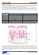
9.0 Function Block Diagram: ...........................................................................................................11
9.1 512MB, 64Mx64 Module (Populated as 1 rank of x16 DDR3 SDRAMs) ................................................11
9.2 1GB, 128Mx64 Module (Populated as 1 rank of x8 DDR3 SDRAMs) ...................................................12
9.3 1GB, 128Mx72 ECC Module (Populated as 1 rank of x8 DDR3 SDRAMs) ............................................13
9.4 2GB, 256Mx64 Module (Populated as 2 ranks of x8 DDR3 SDRAMs) .................................................14
9.5 2GB, 256Mx72 ECC Module (Populated as 2 ranks of x8 DDR3 SDRAMs) ..........................................15
10.0 Absolute Maximum Ratings .....................................................................................................16
10.1 Absolute Maximum DC Ratings ..................................................................................................16
10.2 DRAM Component Operating Temperature Range ........................................................................16
11.0 AC & DC Operating Conditions ...............................................................................................16
11.1 Recommended DC Operating Conditions (SSTL - 15) ....................................................................16
12.0 AC & DC Input Measurement Levels .......................................................................................17
12.1 AC & DC Logic Input Levels for Single-ended Signals ...................................................................17
12.2 V
REF
Tolerances .......................................................................................................................18
12.3 AC & DC Logic Input Levels for Differential Signals ......................................................................19
12.3.1 Differential Signals Definition ..............................................................................................19
12.3.2 Differential Swing Requirement for Clock (CK - CK) and Strobe (DQS - DQS) ............................19
12.3.3 Single-ended Requirements for Differential Signals ...............................................................20
12.3.4 Differential Input Cross Point Voltage ...................................................................................21
12.4 Slew Rate Definition for Single-ended Input Signals ......................................................................21
12.5 Slew Rate Definition for Differential Input Signals .........................................................................21
13.0 AC & DC Output Measurement Levels ....................................................................................22
13.1 Single-ended AC & DC Output Levels ..........................................................................................22
13.2 Differential AC & DC Output Levels .............................................................................................22
13.3 Single-ended Output Slew Rate ..................................................................................................22
13.4 DIfferential Output Slew Rate ....................................................................................................23
Table Contents