
Datasheet

Rev. 1.0 July 2008
DDR2 SDRAM
RDIMM
2 of 26
1.0 DDR2 Registered DIMM Ordering Information ..........................................................................4
2.0 Features ........................................................................................................................................4
3.0 Address Configuration ................................................................................................................4
4.0 Pin Configurations (Front side/Back side) ................................................................................5
5.0 Pin Description ............................................................................................................................5
6.0 Input/Output Functional Description .........................................................................................6
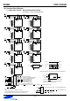
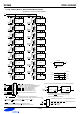
7.0 Functional Block Diagram ...........................................................................................................7
7.1 512MB, 64Mx72 Module - M393T6553GZ3/M393T6553GZA ...............................................................7
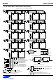
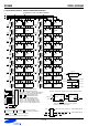
7.2 1GB, 128Mx72 Module - M393T2953GZ3/M393T2953GZA ..................................................................8
7.3 1GB, 128Mx72 Module - M393T2950GZ3/M393T2950GZA ..................................................................9
7.4 2GB, 256Mx72 Module - M393T5750GZ3/M393T5750GZA ................................................................10
8.0 Absolute Maximum DC Ratings ................................................................................................11
9.0 AC & DC Operating Conditions ................................................................................................11
9.1 Recommended DC Operating Conditions (SSTL - 1.8) ....................................................................11
9.2 Operating Temperature Condition ...............................................................................................12
9.3 Input DC Logic Level .................................................................................................................12
9.4 Input AC Logic Level ..................................................................................................................12
9.5 AC Input Test Conditions ...........................................................................................................12
10.0 IDD Specification Parameters Definition ...............................................................................13
11.0 Operating Current Table : .......................................................................................................14
11.1 M393T6553GZ3 / M393T6553GZA : 512MB(64Mx8 *9) Module ....................................................14
11.2 M393T6553GZ3 / M393T6553GZA : 512MB(64Mx8 *9) Module ....................................................14
11.3 M393T2953GZ3 / M393T2953GZA : 1GB(64Mx8 *18) Module ......................................................15
11.4 M393T2953GZ3 / M393T2953GZA : 1GB(64Mx8 *18) Module ......................................................15
11.5 M393T2950GZ3 / M393T2950GZA : 1GB(128Mx4 *18) Module ....................................................16
11.6 M393T2950GZ3 / M393T2950GZA : 1GB(128Mx4 *18) Module ....................................................16
11.7 M393T5750GZ3 / M393T5750GZA : 2GB(128Mx4 *36) Module ....................................................17
11.8 M393T5750GZ3 / M393T5750GZA : 2GB(128Mx4 *36) Module ....................................................17
12.0 Input/Output Capacitance .......................................................................................................18
13.0 Electrical Characteristics & AC Timing for DDR2-800/667/533/400 .....................................18
13.1 Refresh Parameters by Device Density ...................................................................................18
13.2 Speed Bins and CL, tRCD, tRP, tRC and tRAS for Corresponding Bin .........................................18
13.3 Timing parameters by speed grade (DDR2-800 and DDR2-667)....................................................19
13.4 Timing parameters by speed grade (DDR2-533 and DDR2-400)....................................................21
14.0 Physical Dimensions ...............................................................................................................23
14.1 64Mbx8 based 64Mx72 Module (1 Rank) ..................................................................................23
14.2 64Mbx8/128Mbx4 based 128Mx72 Module (2/1 Ranks) ...............................................................24
14.3 128Mbx4 based 256Mx72 Module (2 Ranks) .............................................................................25
15.0 240 Pin DDR2 Registered DIMM Clock Topology .................................................................26
Table of Contents