
Datasheet

Rev. 1.0 July 2008
DDR2 SDRAM
RDIMM
4 of 26
Note :
1. “Z” of Part number(11th digit) stands for Lead-Free and RoHS compliant products.
2. “3” of Part number(12th digit) stands for Dummy Pad PCB products.
3. “A” of Part number(12th digit) stands for Parity Register products.
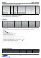
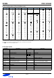
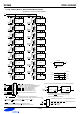
Part Number Density Organization Component Composition Number of Rank Parity Register Height
M393T6553GZ3-CD5/CC 512MB 64Mx72 64Mx8(K4T51083QG)*9EA 1 X 30.00mm
M393T6553GZA-CF7/E6 512MB 64Mx72 64Mx8(K4T51083QG)*9EA 1 O 30.00mm
M393T2953GZ3-CD5/CC 1GB 128Mx72 64Mx8(K4T51083QG)*18EA 2 X 30.00mm
M393T2953GZA-CF7/E6 1GB 128Mx72 64Mx8(K4T51083QG)*18EA 2 O 30.00mm
M393T2950GZ3-CD5/CC 1GB 128Mx72 128Mx4(K4T51043QG)*18EA 1 X 30.00mm
M393T2950GZA-CF7/E6 1GB 128Mx72 128Mx4(K4T51043QG)*18EA 1 O 30.00mm
M393T5750GZ3-CD5/CC 2GB 256Mx72 128Mx4(K4T51043QG)*36EA 2 X 30.00mm
M393T5750GZA-CF7/E6 2GB 256Mx72 128Mx4(K4T51043QG)*36EA 2 O 30.00mm
• Performance range
• JEDEC standard V
DD
= 1.8V ± 0.1V Power Supply
•V
DDQ
= 1.8V ± 0.1V
• 200 MHz f
CK
for 400Mb/sec/pin, 267MHz f
CK
for 533Mb/sec/pin, 333MHz f
CK
for 667Mb/sec/pin, 400MHz f
CK
for 800Mb/sec/pin
•4 Banks
• Posted CAS
• Programmable CAS Latency: 3, 4, 5, 6
• Programmable Additive Latency: 0, 1 , 2 , 3, 4 and 5
• Write Latency(WL) = Read Latency(RL) -1
• Burst Length: 4 , 8(Interleave/Nibble sequential)
• Programmable Sequential / Interleave Burst Mode
• Bi-directional Differential Data-Strobe (Single-ended data-strobe is an optional feature)
• Off-Chip Driver(OCD) Impedance Adjustment
• On Die Termination with selectable values(50/75/150 ohms or disable)
• Average Refresh Period 7.8us at lower than a T
CASE
85°C, 3.9us at 85°C < T
CASE
< 95 °C
- Support High Temperature Self-Refresh rate enable feature
• Serial presence detect with EEPROM
• DDR2 SDRAM Package: 60ball FBGA - 128Mx4/64Mx8
• All of base components are Lead-Free, Halogen-Free, and RoHS compliant
Note: For detailed DDR2 SDRAM operation, please refer to Samsung’s Device operation & Timing diagram.
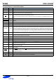
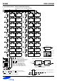
F7(DDR2-800) E6(DDR2-667) D5(DDR2-533) CC(DDR2-400) Unit
Speed@CL3 - 400 400 400 Mbps
Speed@CL4 533 533 533 400 Mbps
Speed@CL5 667 667 533 - Mbps
Speed@CL6 800 - - - Mbps
CL-tRCD-tRP 6-6-6 5-5-5 4-4-4 3-3-3 CK
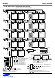
Organization Row Address Column Address Bank Address Auto Precharge
128Mx4(512Mb) based Module A0-A13 A0-A9,A11 BA0-BA1 A10
64Mx8(512Mb) based Module A0-A13 A0-A9 BA0-BA1 A10
1.0 DDR2 Registered DIMM Ordering Information
2.0 Features
3.0 Address Configuration