
Laptop User Manual


CLOCK & POWER MANAGEMENT S3C2440A RISC MICROPROCESSOR
7-22
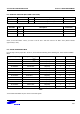
CLOCK CONTROL REGISTER (CLKCON)
Register Address R/W Description Reset Value
CLKCON 0x4C00000C R/W Clock generator control register 0xFFFFF0
CLKCON Bit Description Initial State
AC97 [20] Control PCLK into AC97 block.
0 = Disable, 1 = Enable
1
Camera [19] Control HCLK into Camera block.
0 = Disable, 1 = Enable
1
SPI [18] Control PCLK into SPI block.
0 = Disable, 1 = Enable
1
IIS [17] Control PCLK into IIS block.
0 = Disable, 1 = Enable
1
IIC [16] Control PCLK into IIC block.
0 = Disable, 1 = Enable
1
ADC(&Touch Screen) [15] Control PCLK into ADC block.
0 = Disable, 1 = Enable
1
RTC [14] Control PCLK into RTC control block.
Even if this bit is cleared to 0, RTC timer is alive.
0 = Disable, 1 = Enable
1
GPIO [13] Control PCLK into GPIO block.
0 = Disable, 1 = Enable
1
UART2 [12] Control PCLK into UART2 block.
0 = Disable, 1 = Enable
1
UART1 [11] Control PCLK into UART1 block.
0 = Disable, 1 = Enable
1
UART0 [10] Control PCLK into UART0 block.
0 = Disable, 1 = Enable
1
SDI [9] Control PCLK into SDI interface block.
0 = Disable, 1 = Enable
1
PWMTIMER [8] Control PCLK into PWMTIMER block.
0 = Disable, 1 = Enable
1
USB device [7] Control PCLK into USB device block.
0 = Disable, 1 = Enable
1
USB host [6] Control HCLK into USB host block.
0 = Disable, 1 = Enable
1
LCDC [5] Control HCLK into LCDC block.
0 = Disable, 1 = Enable
1
NAND Flash Controller [4] Control HCLK into NAND Flash Controller block.
0 = Disable, 1 = Enable
1
SLEEP [3] Control SLEEP mode of S3C2440A.
0 = Disable, 1 = Transition to SLEEP mode
0
IDLE BIT [2] Enter IDLE mode. This bit is not cleared automatically.
0 = Disable, 1 = Transition to IDLE mode
0
Reserved [1:0] Reserved 0