
Laptop User Manual


S3C2440A RISC MICROPROCESSOR PRODUCT OVERVIEW
1-27
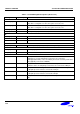
S3C2440A SPECIAL REGISTERS
Table 1-4. S3C2440A Special Registers (Sheet 1 of 14)
Register
Name
Address
(B. Endian)
Address
(L. Endian)
Acc.
Unit
Read/
Write
Function
Memory Controller
BWSCON 0x48000000
←
W R/W Bus Width & Wait Status Control
BANKCON0 0x48000004 Boot ROM Control
BANKCON1 0x48000008 BANK1 Control
BANKCON2 0x4800000C BANK2 Control
BANKCON3 0x48000010 BANK3 Control
BANKCON4 0x48000014 BANK4 Control
BANKCON5 0x48000018 BANK5 Control
BANKCON6 0x4800001C BANK6 Control
BANKCON7 0x48000020 BANK7 Control
REFRESH 0x48000024 DRAM/SDRAM Refresh Control
BANKSIZE 0x48000028 Flexible Bank Size
MRSRB6 0x4800002C Mode register set for SDRAM BANK6
MRSRB7 0x48000030 Mode register set for SDRAM BANK7