Evaluation Board Manual S3F401F 16/32-BIT RISC MICROPROCESSOR Dec, 2007 REV 1.
Table of Contents Chapter 1 Evaluation Board Manual 1. Overview ...................................................................................................................................................... 1 1.1 Features................................................................................................................................................ 3 1.2 System Requirements ..............................................................................................................
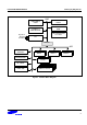
EVALUATION BOARD MANUAL 1 S3F401F_BD_UM_REV1.00 EVALUATION BOARD MANUAL 1. OVERVIEW S3F401F EVB (Evaluation Board) is a compact platform that is suitable for code development of SAMSUNG's S3F401F 16-/32-bit RISC microcontroller for an inverter motor and general purpose application. EVB is consists of several blocks, which can make operate the function of S3F401F.
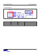
EVALUATION BOARD MANUAL S3F401F_BD_UM_REV1.00 AHB FLASH-ROM 256KB ARM7TDMI-S CORE SRAM 20KB INTERRUPT CONTROLLER Crystal or Ceramic Oscillator TAP CONTROLLER For JTAG PLL BRIDGE APB CLOCK MONITOR I/O CONTROLLER IMC0/1 IMC0/1 ENC0/1 ENC0/1 UART0/1 UART0/1 SSP0/1 SSP0/1 BT & WDT 12-BIT ADC Timer0/1/2/3/4/5 Timer0/1/2/3/4/5 Timer0/1/2/3/4/5 Timer0/1/2/3/4/5 TIMER 0/1/2/3/4/5 Figure 1.
EVALUATION BOARD MANUAL 1.1 S3F401F_BD_UM_REV1.00 FEATURES Micro-Controller S3F401F, ARM7TDMIS, 16/32-bit RISC Microcontroller Board Power Source External DC 7~12V Adjustable voltage regulator out is 3.
EVALUATION BOARD MANUAL S3F401F_BD_UM_REV1.00 1.3 BOARD COMPONENTS The board consists of the followings. S3F401F Micro-controller 64LC40S and X25650 as a serial EEPROM for SSP 2 x DSUB Connector for RS-232 2 x Header groups for IMC function 1 x Buzzer 6 x Switches: IRQ x 2, Power, Reset 4 x LED: Power x1, IO Port output x 3 A regulator to generate 3.
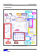
EVALUATION BOARD MANUAL S3F401F_BD_UM_REV1.00 2. CONFIGURATION IMC1 HEADER CONNECTOR Page 1-11 SSP BLOCK JTAG 12-bit ADC BLOCK MODE SETTING BLOCK Page 1 -12 Page 1-7 Buzzer Page 1-9 S3F401FX Main OSC POWER BLOCK 7-SEGMENT IMC0 HEADER CONNECTOR UART BLOCK Page 1-6 Page 1-10 Page 1-11 Page 1-8 Figure 2.
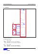
EVALUATION BOARD MANUAL S3F401F_BD_UM_REV1.00 2.1 DETAILED BLOCK CONFIGURATIONS 2.1.1 Power Block 5 4 2 1 3 ① CN1, CN2, J23: Power Supply Connector CN1 : VIN CN2 : GND J23 : DC adapter connector ② U7: Adjustable Voltage Regulator 3.3V generator J VDD33, VDDCORE, VDDIO ③ SW6: Power Switch ④ DS4: Power Display LED VDD33 Power-on status display ⑤ J22: Jumper Setting Selection VDDCORE / VDDIO 1-2 connection: The VDD of each block is connected to VDD33.
EVALUATION BOARD MANUAL S3F401F_BD_UM_REV1.00 2.1.
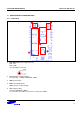
EVALUATION BOARD MANUAL S3F401F_BD_UM_REV1.00 2.1.3 UART Block 2 ④ 1 3 ① U10, U11: UART Driver IC ② P2, P3: UART Connector ③ J25 TXD0 RXD0 Jumper Setting UARTTXD0 is connected to T1IN of MAX3221. UARTRXD0 is connected to R1OUT of MAX3221. ④ J26 TXD1 RXD1 Jumper Setting UARTTXD1 is connected to T1IN of MAX3221 UARTRXD1 is connected to R1OUT of MAX3221.
EVALUATION BOARD MANUAL S3F401F_BD_UM_REV1.
EVALUATION BOARD MANUAL S3F401F_BD_UM_REV1.00 2.1.4 SSP Block 1 2 ① U9: SSP8 serial EEPROM (8K × 8bit) SW9 ON FSS0 is connected to P1.16. RXD0 is connected to P1.14. SW10 ON CLK0 is connected to P1.15. TXD0 is connected to P1.13. ② U8: SSP16 serial EEPROM (4K × 16bit) SW7 ON FSS1 is connected to P1.20. CLK1 is connected to P1.19. RXD1 is connected to P1.18. TXD1 is connected to P1.17. SW8 ON The RDY/nBUSY pin is connected to P2.11. The RESET pin is connected to P2.10.
EVALUATION BOARD MANUAL S3F401F_BD_UM_REV1.
EVALUATION BOARD MANUAL 2.1.5 S3F401F_BD_UM_REV1.00 7-SEGMENT BLOCK 1 2 3 The assignment of 7-segment control pins on the S3F401F-EVB is the same like this. ① SW1 ON: This Port (P0.0~P0.7) is connected to each segment of 7-segment. ② SW2 ON: This Port (P1.9~P1.12) is connected to latch.
EVALUATION BOARD MANUAL 2.1.6 S3F401F_BD_UM_REV1.00 IMC BLOCK 1 2 The assignment of IMC pins on the S3F401F-EVB is the same like this.
EVALUATION BOARD MANUAL 2.1.7 S3F401F_BD_UM_REV1.00 ADC BLOCK ⑥ 2 3 4 5 1 ① J1: ADC input connector ② J2, J3, J4: J2, J3 and J4 are selected to sample test with AIN0, AIN1 and AIN2 ③ RV1: Variable Resistor ④ J24: ADC Power Source Close: When connecting (short), AVDD is same to VDD33. Open: AVDD is a second (right) pin of J24. So, AVDD should be connected to another power. ⑤ J7: 2,3 connection - ADTRG signal is generated by SW4 ⑥ SW11, SW12: Control cap for each ADC input port.
EVALUATION BOARD MANUAL S3F401F_BD_UM_REV1.00 3. TOTAL BLOCKS’ UNIT & JUMPER SUMMURY 3.1 FUNCTION BLOCKS Block Symbols 7-SEGMENT U3 4Digit Segment IMC J20 MOTOR 1 J21 MOTOR 2 U14 RS-232 transceiver P41 RS-232 connector U7 SPI8 interface EEPROM (8K × 8bit) U8 SPI16 interface EEPROM (4K × 16bit) J28 SPI block pin assignment POWER U11 3.
EVALUATION BOARD MANUAL S3F401F_BD_UM_REV1.00 3.2 JUMPER CONNECTION JP# Description Default Setting AIN0~AIN14 − J1 ADC block pin assignment J2 AIN0 input voltage connector Connect (Short) J3 AIN1 input voltage connector Connect (Short) J4 AIN2 input voltage connector Connect (Short) J5 SW3_INPUT VDDIO connects to INT7 J6 Buzzer connector T3PWM connects to Buzzer J7 SW4_INPUT VDDIO connects to INT8 J8 LED signal connector Port 0.0/0.1/0.
EVALUATION BOARD MANUAL S3F401F_BD_UM_REV1.00 3.2 JUMPER CONNECTION (Continued) JP# J9 Description Default Setting J9 J10 J11 MD[1:0] J10 2-3 2-3 2-3 NORMAL J11 1-2 2-3 2-3 SPGM MODE selection All 2-3 connect :Normal Mode J12 Port assignment pin Port 2 Open J13 Port assignment pin Port 1 Open J14 Port assignment pin Port 0 Open J15 nTRST The JTAG connects to nTRST Open J16 Chip socket connection Chip socket board is connected with S3F401F-EVB.
EVALUATION BOARD MANUAL S3F401F_BD_UM_REV1.00 3.3 SWITCHES SW# Description SW1 7-Segment ON: Port 0.0~0.7 connects to 7segment SW2 Latch ON: Port 1.9~1.
EVALUATION BOARD MANUAL S3F401F_BD_UM_REV1.00 4. S3F401F-EVB REV 1.0 BOARD SCHEMATICS SCH-01 EVB TOP Block Diagram REV 1.0 SCH-02 S3F401F Micro-Controller REV 1.0 SCH-03 System Power Generation REV 1.0 SCH-04 Clock & Mode REV 1.0 SCH-05 ADC, Interrupt & BUZZER REV 1.0 SCH-06 JTAG Connector REV 1.0 SCH-07 UART Communication REV 1.0 SCH-08 SSP Communication REV 1.0 SCH-09 IMC & ENC Signal REV 1.0 SCH-10 7-Segment Display REV 1.0 SCH-11 Expansion Connector REV 1.
S3F401F_BD_UM_REV1.
S3F401F_BD_UM_REV1.
S3F401F_BD_UM_REV1.
S3F401F_BD_UM_REV1.
S3F401F_BD_UM_REV1.
S3F401F_BD_UM_REV1.
S3F401F_BD_UM_REV1.
S3F401F_BD_UM_REV1.
S3F401F_BD_UM_REV1.
S3F401F_BD_UM_REV1.
S3F401F_BD_UM_REV1.