
User`s manual

DEVELOPMENT TOOLS S3F84A5_UM_REV1.10
21-4
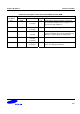
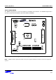
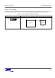
Table 21-1. Components of TB84A5
Symbols Usage Description
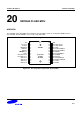
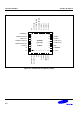
J1 100-pin connector Connection between emulator and TB84A5 target board.
J2 40-pin connector Connection between target board and user application
system
RESET Push button Generation low active reset signal to S3F84A5 EVA-chip
VDD, GND Power connector External power connector for TB84A5
IDLE, STOP LED STOP/IDLE Display Indicate the status of STOP or IDLE of S3F84A5 EVA-chip
on TB84A5 target board
JP1 Operation Mode Selection Selection of RUN/Test mode
JP2 SMDS2+ Selection Selection of SMDS2/SMDS2+
JP3 User’s Power Selection Selection of User_VCC (Power to User)
JP6 Clock Source Selection Selection of SMDS2/SMDS2+ internal /external clock
JP7 MODE Selection Selection of Eva/Main-chip mode
JP8 PWM Selection Selection of PWM enable/disable mode
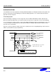
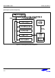
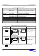
Table 21-2. Power Selection Settings for TB84A5
"To User_Vcc"
Settings
Operating Mode Comments
To user_Vcc
off
on
Target
System
SMDS2/SMDS2+
TB84A5
VCC
VSS
VCC
External
The SMDS2/SMDS2+ main
board supplies V
CC
to the
target board (evaluation chip)
and the target system.
on
To user_Vcc
off
Target
System
SMDS2/SMDS2+
TB84A5
VCC
VSS
VCC
External
The SMDS2/SMDS2+ main
board supplies V
CC
only to the
target board (evaluation chip).
The target system must have
its own power supply.
NOTE: The following symbol in the "To User_Vcc" Setting column indicates the electrical short (off) configuration: