
User`s manual


S3F84A5_UM_REV1.10 CONTROL REGISTER
4-1
4 CONTROL REGISTERS
OVERVIEW
Control register descriptions are arranged in alphabetical order according to register mnemonic. More detailed
information about control registers is presented in the context of the specific peripheral hardware descriptions in
Part II of this manual.
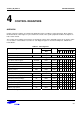
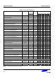
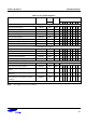
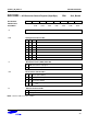
The locations and read/write characteristics of all mapped registers in the S3F84A5 register file are listed in Table
4-1, 4-2 and 4-3. The hardware reset value for each mapped register is described in Chapter 8, “RESET and
Power-Down".
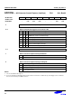
Table 4-1. Set 1 Registers
Register Name Mnemonic Address R/W RESET Values (bit)
Hex 7 6 5 4 3 2 1 0
Location D0H is not mapped
STOP control register STPCON D1H R/W 0 0 0 0 0 0 0 0
Location D2H is not mapped
Basic timer control register BTCON D3H R/W 0 0 0 0 0 0 0 0
System clock control register CLKCON D4H R/W – – – 0 0 – – –
System flags register FLAGS D5H R/W x x x x x x 0 0
Register pointer 0 RP0 D6H R/W 1 1 0 0 0 – – –
Register pointer 1 RP1 D7H R/W 1 1 0 0 1 – – –
Location D8H is not mapped
Stack pointer (low Byte) SPL D9H R/W x x x x x x x x
Instruction pointer (high Byte) IPH DAH R/W x x x x x x x x
Instruction pointer (low Byte) IPL DBH R/W x x x x x x x x
Interrupt request register IRQ DCH R 0 0 0 0 0 0 0 0
Interrupt mask register IMR DDH R/W x x x x x x x x
System mode register SYM DEH R/W 0 – – x x x 0 0
Register page pointer PP DFH R/W 0 0 0 0 0 0 0 0
NOTE: – : Not mapped or not used, x: Undefined.