GSM TELEPHONE SGH-C140i GSM TELEPHONE CONTENTS 1. Specification 2. Exploded View and Parts List 3. Flow Chart of Troubleshooting 4. Array course control 5. Block Diagrams 6. PCB Diagrams 7. MAIN Electrical Parts List 8. Reference data 9. Safety Precautions 10.
Contents 1. Specification 1-1. GSM General Specification .......................................................................................1-1 1-2. GSM Tx Power Class ...............................................................................................1-2 2. Exploded View and Parts List 2-1. Cellular phone Exploded View ..................................................................................2-1 2-2. Cellular phone Part list ...........................................................
Contents 5. MAIN Electrical Parts List 6. Block Diagrams 7. PCB Diagrams 8. Reference data 9. Safety Precautions 9-1. Repair Precaution ......................................................................................................9-1 9-2. ESD(Electrostatically Sensitive Devices) Precaution ...............................................9-2 10. Product Function 10-1. Main Function .........................................................................................................
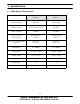
1. Specification 1-1. GSM General Specification EG SM 9 00 Ph ase 2 DCS1 800 Phase 1 F req. Ban d[MHz] Uplin k/Down link 8 80~915 9 25~960 1710~1 785 1805~1 880 ARF CN ra nge 0~1 24 & 9 75~102 3 512~8 85 T x/Rx spacing 45 M Hz 95 MHz Mo d. Bit r ate/ Bit Period 270 .833 kb ps 3 . 692 u s 2 70.83 3 kbps 3.69 2 us Ti me Slo t Pe rio d/Fr am e Per iod 5 76.9 u s 4. 615 ms 576. 9 us 4 .615 ms Modula tion 0 .3 G M SK 0.
Speclflcation 1-2.
2. Exploded View and Parts List 2-1.
Main Electrical Parts List 2-2.
Main Electrical Parts List Discription SEC CODE BAG PE 6902-000634 ADAPTOR-SGHC140 DC JACK (INDA_ GH44-01622A MANUAL-SFC CARD(INDA) GH68-08768A LABEL(R)-WATER SOAK GH68-09361A MANUAL USERS-INDA LEAFLET CARD GH68-13751A MANUAL USERS-INDA ENGLISH GH68-14750A LABEL(R)-MAIN(EU) GH68-14912A BOX(P)-UNIT MAIN(INU) GH69-05476H NPR-BRACKET LID GH71-07160A MPR-TAPE CAM CON MASK GH74-18424A MPR-SPONGE SPK A GH74-28347A MPR-SPONGE SPK B GH74-28350A MPR-VINYL BOHO WINDOW GH74-30206A MPR-TAPE
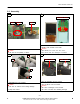
Main Electrical Parts List 2-3. Assembly 1 2 Standard Points Motor Speaker Mike 1) Attach the LCD module to the PBA. 2) Solder LCD module to the PBA. 1) Solder the motor, speaker and mike. ※ caution ※ caution 1) Be careful, the motor wire isn’t down. 2) Be careful with the damages of FPCBS. 1) Be care of the polarity of wires. 3 4 2 Rotate 3 times 1 Rotate 1 time 4 3 1) Assemble the LCD module. ※ caution 1) Be care of scratch and molding damage. 2) Keep the orders.
Main Electrical Parts List 6 5 2 3 1 1) Assemble the LCD module. ※ caution 1) Check the PBA 1) Be care of scratch and molding damage. 2) Keep the orders. ※ caution 1) Be care of scratch and molding damage. 8 7 Put the left side of the PBA 1 Press right side of the PBA. 2 Push the back of MIC to attach firmly. 1) Put the PBA to the FRONT 1) Screw down 4 Points ※ caution ※ caution 1) Be care of scratch and molding damage. 1) Be care of scratch and molding damage.
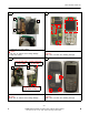
Main Electrical Parts List 2-4. Disassembly 2 1 1) Unscrew the 4 points. 2) Separate the REAR from the FRONT using an assembly stick. ※ caution 1) Be care of scratch and molding damage. 1) Disassemble the FRONT from the PBA. ※ caution 1) Be care of scratch and molding damage. 2) Be care of damage to the PBA. 4 3 2 1 3 Check the MIC holder. It could be lost easily. 1) Disassemble the Carrier from the PBA. 1) Check the FRONT. ※ caution ※ caution 1) Be care of damage to the wires.
Main Electrical Parts List 5 6 3 4 1 2 1) Detach the Speaker and Motor from the Carrier using tweezers. ※ caution 1) Be care of scratch and molding damage. 2) Be care of damage to the wires. 7 1) Disassemble the LCD module from the PBA ※ caution 1) Be care of scratch and molding damage. 2) Be care of damage to the LCD module. Soldering Points 1) Solder the LCD FPCB to take the LCD out. ※ caution 1) Be care of scratch and molding damage. 2) Be care of damage to the LCD FPCB.
3. Flow Chart of Troubleshooting 3-1. Baseband 3-1-1. Power ON 'Power ON' does not work check the current consumption >= 100mA No Download again Yes Check the Voltage of the Battery >= 3.3V No Charge the battery Yes Check the pin C100,C101,C102 of UCP101 is >= 2.8V >=2.
C100 DSP_DB(15) DSP_DB(14) DSP_DB(13) DSP_DB(12) DSP_DB(11) DSP_DB(10) DSP_DB(9) D2 D3 E3 E2 F3 F2 F1 DB15 DB14 DB13 DB12 DB11 DB10 3-2 B4 C4 P13 L11 F6 A6 M10 N11 P6 R2 K4 G5 J4 N5 N6 M3 J3 F11 K15 B15 E8 B13 C10 2 1 K10 J10 J9 J8 J7 H9 H8 H7 H6 G10 G9 G8 G7 F10 F9 F8 F7 D13 VCCD_2.
Flow Chart of Troubleshooting 3-1-2. Initial Initial Failure No check the pin RSTB of UCP201 is LOW? Check UCP201 1 Yes No check the pin CKI of UCP201 is 13Mhz? Check R308, R306, C341 2 Yes Check the clock signal No at pin #3 of OSC400 check OSC400 3 Freq=26Mhz? Yes Check VCCD_2.9V, VCCD_1.
3-4 G16 F10 E10 C11 D8 F17 C12 E15 B14 E17 E16 N16 U16 U15 P8 U2 M1 B1 C16 A5 R17 R16 T13 R4 R1 G1 E2 L9 J11 L8 M7 L10 L6 K7 K6 J7 H11 H7 G10 G9 F6 A3 A2 C204 VSS_DPLL VDD_DPLL XVREF VSSA VDDA VRTC CKI RSTB VDDE VDDE VDDE VDDE VDDE VDDE VDDE VDDE VDDE VDDE VDD VDD VDD VDD VDD VDD VDD VDD VDD VSS VSS VSS VSS VSS VSS VSS VSS VSS VSS VSS VSS VSS VSS VSS VSS Flow Chart of Troubleshooting VCCD_1.8V R202 VCCD_2.9V C205 3 4 2 1 VRTC_3V C206 TDO TRST TDI TMS TCK C207 VCCD_1.8V VCCD_2.
Flow Chart of Troubleshooting 3-1-3. Sim Part "Insert SIM" is displayed on the LCD No The voltage is 2.
Flow Chart of Troubleshooting 3-1-4.Microphone Part * Call with Sim before testing. MicroPhone does not work Yes No Check the soldered status of microphone Resolder microphone Yes Check the reference voltage on mic path C139 ≒ 2.0V Resolder or change R143,R147,C139,C145,C140,C144, R148,R149,R150,R152 No 1 Yes No Is microphone OK? Check UCP101 2 Yes VCCA_2.
Flow Chart of Troubleshooting 1 2 1 3-7
Flow Chart of Troubleshooting 3-1-5. Speaker Part There is no sound from speaker No Is the terminal of Speaker O.K.
Flow Chart of Troubleshooting 1 ③ 2 3-9
Flow Chart of Troubleshooting 3-1-6. LCD backlight Backlight does not work No Backlight ON "TIME" mode in the menu? Select backlight "15 sec" mode Yes No Check conecting between PBA and LCD conector Check FPCB Yes Check MOD300 △v(pin #26 - #28,29) = 3.1/2.
Flow Chart of Troubleshooting VBAT VCCD_2.
Flow Chart of Troubleshooting 3-2. RF 3-2-1. GSM Rx CONTINOUS RX ON RF INPUT : 62CH AMP : -50dbm Normal condition catch the channel ? No Check ANT, C303, R300 1 Yes Check PAM400 pin 12 ≥ -65 dbm ? No Resolder or change RFS400, L300, L301, L303, C305, C302 2 No Resolder or change PAM400 3 No Resolder or change F401, C319, U409, L306 4 Resolder or change UCP101 5 Yes Check PAM400 pin 16 ≥ -65 dbm ? Yes Check U400 pin 21,22 ≥65dBm ? Yes Check U400 pin 13 = 2.
Flow Chart of Troubleshooting 1 2 3 4 5 3-13
Flow Chart of Troubleshooting 3-2-2. DCS Rx CONTINOUS RX ON RF INPUT : 698CH AMP : -50dbm Normal condition catch the channel ? No Check ANT, C303, R300 1 Yes Check PAM400 pin 12 ≥ -65 dbm ? No Resolder or change RFS400, L300, L301, L303, C305, C302 2 No Resolder or change PAM400 3 No Resolder or change F400, C310, C312, L304 No Resolder or change UCP101 Yes Check PAM400 pin 18 ≥ -65 dbm ? Yes Check U400 pin 19,20 ≥65dBm ? 4 Yes Check U400 pin 13 = 2.
Flow Chart of Troubleshooting 1 2 3 4 5 3-15
TP102 TP101 3-16 TX_EN BAND_SEL1 GSM_LNA_IN_P GSM_LNA_IN_N DCS_LNA_IN_P DCS_LNA_IN_N DPCS_PAM_IN GSM_PAM_IN L302 R300 C304 U409 C319 C312 C310 C303 L306 L304 G 4 G 2 G 5 3 OUT 4 OUT 2 F401 G 5 F400 G 3 OUT 4 OUT C 3 A 2 G 1 RFS400 IN IN 1 1 L303 L301 C311 C317 C329 C305 1 6 4 16 20 11 C330 L300 VTX VBS RX2 RX1 ANT PAM400 12 5 13 15 17 19 VRAMP V1 VCC2 VCC1 VBATT 21 NC NC VMOD_EN GND GND GND GND GND GND GSM900_IN DCSIN C358 C302 18
Flow Chart of Troubleshooting VRF_2.9V 3 4 HOT GND2 C301 C300 OSC400 GND1 HOT 2 1 26M_OUT RTXQN AFC RTXQP R301 C307 VCCD_2.
Flow Chart of Troubleshooting 3-2-3. GSM Tx CONTINUS TX ON CONDITION 2 Check U400pin 15 : about 2~3 dbm? No Yes Yes 1 Check and change RFS400, L300,L301 TX POWER DAC : 554 CODE APPLIED CH : 62ch RBW : 100KHz VBW : 100KHz SPAN : 10MHz REF LEV : 10dBm ATT : 20dB Check and change UCP201,UCP101 No Check U400 pin 6 : 2.8V ? No PAM400 pin 11: about 4~5dbm? Yes U400 check & change PAM400 pin 7 : 3.7V ? No 1 3 Battery, UCP101 check & change 4 3 7 Yes PAM400 pin 8 : 1.
Flow Chart of Troubleshooting 3-2-4. DCS Tx CONTINUS TX ON CONDITION Check U400 pin 16 : about 2~3 dbm? No Yes 1 No Check U400 pin 6 : 2.8V ? No VBW : 100KHz SPAN : 10MHz REF LEV : 10dBm ATT : 20dB 2 Yes Check and change RFS400, L300,L301 TX POWER DAC : 560 CODE APPLIED Check and change CH : 698CH(DCS), 660CH(PCS) UCP201,UCP101 RBW : 100KHz PAM400 pin 1 : about 4~5dbm? Yes U400 check & change PAM400 pin 7 : 3.7V ? No 3 1 Battery, PAM400 4 check & change Yes PAM400 pin 8 : 1.
4.
Array course control Software Downloadin 4-1. Downloading Binary Files • Three binary files for downloading C140i. – C140iXXYY.s3 : Main source code binary. 4-2. Pre-requsite for Downloading • Downloader Program(OptiFlash.
Array course control 4-3. S/W Downloader Program 1. Load the binary download program by executing the “OptiFlash.exe” 2. Select the “Options” -> “Settings” -> “Generic” -> “Specify hardware platform”. Choose hardware platform for the downloader file setting.
Array course control 3. Select the COM port when the download cable is connected Up to twelve ports are supported. Additionally you can select the maximum transfer speed OptiFlash will use to communicate with the phone.
Array course control 4. Select the“Flash&Verify” -> “Browse” Set the directory path and choose the latest s/w binary, for example C140iXXYY.s3”, for the downloader binary setting. Make sure that not to change the reserved memory regions.
Array course control 5. Click “OK” button then press “Flash”. (Before pressing ‘Flash’ button, push the button ‘*’and ‘END’ at the same time. Then press ‘Flash’.) Downloader will upload the binary file as below for the downloading. 6. When downloading is finished successfully, there is a “All is well” message. 7. After finishing downloading, Certain memory resets should be done to guarantee the normal performance. 8. Confirm the downloaded version name and etc.
5.
6.
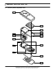
PCB Diagrams MOD300 GND300 GND301 LED301 SEND DOWN VR205 RIGHT STO PWR VR206 ZD217 VR212 CLEAR VR203 1 2 VR204 4 6 5 LED308 7 * 3 VR209 LE D303 LE D302 VR208 8 0 6-2 9 SHARP LED306 VR210 ZD218 LED304 I LED305 ZD216 MENU LED307 LEFT UP
7.
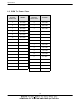
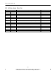
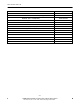
Exploded View and Parts List SEC CODE Design LOC Discription STATUS 1405-001082 VR212 VARISTOR SA 1405-001082 ZD216 VARISTOR SA 1405-001082 ZD217 VARISTOR SA 1405-001082 ZD218 VARISTOR SA 2007-000139 R119 R-CHIP SA 2007-000148 R121 R-CHIP SA 2007-000148 R124 R-CHIP SA 2007-000148 R148 R-CHIP SA 2007-000148 R149 R-CHIP SA 2007-000157 R144 R-CHIP SA 2007-000157 R206 R-CHIP SA 2007-000160 R142 R-CHIP SA 2007-000161 R125 R-CHIP SA 2007-000161 R127 R-CHI
Exploded View and Parts List SEC CODE Design LOC Discription STATUS 2007-000172 R122 R-CHIP SA 2007-000172 R200 R-CHIP SA 2007-000172 R204 R-CHIP SA 2007-000172 R312 R-CHIP SA 2007-000172 R313 R-CHIP SA 2007-000172 R314 R-CHIP SA 2007-000172 R315 R-CHIP SA 2007-000172 R316 R-CHIP SA 2007-000172 R317 R-CHIP SA 2007-000172 R318 R-CHIP SA 2007-000172 R319 R-CHIP SA 2007-000242 R120 R-CHIP SA 2007-000242 R133 R-CHIP SA 2007-000242 R147 R-CHIP SA 2007-
Exploded View and Parts List SEC CODE Design LOC Discription STATUS 2007-008403 R207 R-CHIP SA 2007-008403 R212 R-CHIP SA 2007-008419 R107 R-CHIP SA 2007-008419 R108 R-CHIP SA 2007-008419 R115 R-CHIP SA 2007-008516 R303 R-CHIP SA 2007-008542 R214 R-CHIP SA 2007-008579 R143 R-CHIP SA 2007-009160 R156 R-CHIP SA 2203-000233 C101 C-CER,CHIP SA 2203-000233 C218 C-CER,CHIP SA 2203-000254 C100 C-CER,CHIP SA 2203-000254 C136 C-CER,CHIP SA 2203-000254 C202 C
Exploded View and Parts List SEC CODE Design LOC Discription STATUS 2203-000995 C131 C-CER,CHIP SA 2203-001405 C135 C-CER,CHIP SA 2203-001412 C344 C-CER,CHIP SA 2203-002487 C147 C-CER,CHIP SA 2203-002487 C148 C-CER,CHIP SA 2203-002709 C332 C-CER,CHIP SA 2203-005344 C120 C-CER,CHIP SA 2203-005344 C129 C-CER,CHIP SA 2203-005344 C207 C-CER,CHIP SA 2203-005482 C338 C-CER,CHIP SA 2203-005482 C348 C-CER,CHIP SA 2203-005682 C322 C-CER,CHIP SA 2203-005682 C327
Exploded View and Parts List SEC CODE Design LOC Discription STATUS 2203-005819 C123 C-CER,CHIP SA 2203-005819 C125 C-CER,CHIP SA 2203-005819 C352 C-CER,CHIP SA 2203-005819 C353 C-CER,CHIP SA 2203-005819 C354 C-CER,CHIP SA 2203-005819 C355 C-CER,CHIP SA 2203-006048 C102 C-CER,CHIP SA 2203-006048 C111 C-CER,CHIP SA 2203-006048 C118 C-CER,CHIP SA 2203-006048 C121 C-CER,CHIP SA 2203-006048 C122 C-CER,CHIP SA 2203-006048 C124 C-CER,CHIP SA 2203-006048 C132
Exploded View and Parts List SEC CODE Design LOC Discription STATUS 2203-006348 C115 C-CER,CHIP SA 2203-006348 C116 C-CER,CHIP SA 2203-006348 C117 C-CER,CHIP SA 2203-006348 C149 C-CER,CHIP SA 2203-006361 C142 C-CER,CHIP SA 2203-006423 C126 C-CER,CHIP SA 2203-006423 C301 C-CER,CHIP SA 2203-006423 C315 C-CER,CHIP SA 2203-006423 C320 C-CER,CHIP SA 2203-006423 C325 C-CER,CHIP SA 2203-006423 C326 C-CER,CHIP SA 2203-006462 C324 C-CER,CHIP SA 2203-006556 C302
Exploded View and Parts List SEC CODE Design LOC Discription STATUS 2703-002917 L300 INDUCTOR-SMD SA 2703-002917 L301 INDUCTOR-SMD SA 2801-003856 OSC201 CRYSTAL-SMD SA 2801-004587 OSC400 CRYSTAL-SMD SA 2904-001592 F401 FILTER-SAW SA 2904-001599 F400 FILTER-SAW SA 3301-001534 L308 BEAD-SMD SA 3705-001358 RFS400 CONNECTOR-COAXIAL SA 3709-001336 SIM103 CONNECTOR-CARD EDGE SA 3711-006084 BTC104 HEADER-BATTERY SA 3722-001876 DCJ101 JACK-DC POWER SA 3722-002249 EA
8. Reference data 8-1. Reference Abbreviate AAC: Advanced Audio Coding. AVC : Advanced Video Coding.
9. Safety Precautions 9-1. Repair Precaution ● Repair in Shield Box, during detailed tuning. Take specially care of tuning or test, because specipicty of cellular phone is sensitive for surrounding interference(RF noise). ● Be careful to use a kind of magnetic object or tool, because performance of parts is damaged by the influence of manetic force. ● Surely use a standard screwdriver when you disassemble this product, otherwise screw will be worn away. ● Use a thicken twisted wire when you measure level.
Safety Precautions 9-2. ESD(Electrostatically Sensitive Devices) Precaution Several semiconductor may be damaged easilly by static electricity. Such parts are called by ESD(Electrostatically Sensitive Devices), for example IC,BGA chip etc. Read Precaution below. You can prevent from ESD damage by static electricity. ● Remove static electricity remained your body before you touch semiconductor or parts with semiconductor.
10. Product Function Main Function - Network services - SMS & SOS message - Voicemail - Web browser - Calendar, Calculator, Speed dial, etc...
GSPN (Global Service Partner Network) Country North America Latin America CIS Europe China Asia Mideast & Africa This Service Manual is a property of Samsung Electronics Co.,Ltd. Any unauthorized use of Manual can be punished under applicable International and/or domestic law. Web Site service.samsungportal.com latin.samsungportal.com cis.samsungportal.com europe.samsungportal.com china.samsungportal.com asia.samsungportal.com mea.samsungportal.com ⓒ Samsung Electronics Co.,Ltd. 2007. 05. Rev.1.