GSM TELEPHONE SGH-F210 GSM TELEPHONE CONTENTS 1. Safety Precautions 2. Specification 3. Product Function 4. Array course control 5. Exploded View and Parts list 6. MAIN Electrical Parts List 7. Block Diagrams 8. PCB Diagrams 9. Chart of Troubleshooting 10. Reference data 11.
GSPN (Global Service Partner Network) Country Web Site North America service.samsungportal.com Latin America latin.samsungportal.com CIS cis.samsungportal.com Europe europe.samsungportal.com China china.samsungportal.com Asia asia.samsungportal.com Mideast & Africa mea.samsungportal.com This Service Manual is a property of Samsung Electronics Co.,Ltd. Any unauthorized use of Manual can be punished under applicable International and/or domestic law. ⓒ Samsung Electronics Co.,Ltd. 2007. 09. Rev.1.
1. Safety Precautions 1-1. Repair Precaution ● Repair in Shield Box, during detailed tuning. Take specially care of tuning or test, because specipicty of cellular phone is sensitive for surrounding interference(RF noise). ● Be careful to use a kind of magnetic object or tool, because performance of parts is damaged by the influence of manetic force. ● Surely use a standard screwdriver when you disassemble this product, otherwise screw will be worn away. ● Use a thicken twisted wire when you measure level.
Safety Precautions 1-2. ESD(Electrostatically Sensitive Devices) Precaution Several semiconductor may be damaged easilly by static electricity. Such parts are called by ESD(Electrostatically Sensitive Devices), for example IC,BGA chip etc. Read Precaution below. You can prevent from ESD damage by static electricity. ● Remove static electricity remained your body before you touch semiconductor or parts with semiconductor.
2. Specification 2-1. GSM General Specification E- GSM DCS1800 P C S 19 00 Freq. Ban d [M Hz ] Upl in k/Downl in k 88 0~9 15 92 5~9 60 1 71 0~ 1 78 5 1 80 5~ 1 88 0 1 85 0~ 1 91 0 1 93 0~ 1 99 0 A RF C N ra n g e 97 5~ 10 23 0~12 4 51 2~8 85 51 2~8 10 Tx/R x sp aci ng 45 MHz 95 MHz 80 MHz 27 0. 83 3K b ps 3.692us 8 12 . 5 K b p s 3.692us 27 0. 83 3K b ps 3.692us 8 12 . 5 K b p s 3.692us 27 0. 83 3K b ps 3.692us 8 12 . 5 K b p s 3.692us 576.9us 4. 61 5ms 576.9us 4. 61 5ms 576.9us 4.
Speclflcation 2-2.
3.
4.
Array course control Software Downloading 4-1. Downloading Binary Files • Three binary files for downloading F210 – F210XXYY.s3 : Main source code binary. 4-2. Pre-requsite for Downloading • Downloader Program(OptiFlash.
Array course control 4-3. S/W Downloader Program 1. Load the binary download program by executing the “OptiFlash.exe” 2. Select the “Options” -> “Settings” -> “Generic” -> “Specify hardware platform”. Choose hardware platform for the downloader file setting.
Array course control 3. Select the COM port when the download cable is connected Up to twelve ports are supported. Additionally you can select the maximum transfer speed OptiFlash will use to communicate with the phone.
Array course control 4. Select the“Flash&Verify” -> “Browse” Set the directory path and choose the latest s/w binary, for example “XC30XXYY.s3”, for the downloader binary setting. Make sure that not to change the reserved memory regions.
Array course control 5. Click “OK” button then press “Flash”. (Before pressing ‘Flash’ button, push the button ‘*’and ‘END’ at the same time. Then press ‘Flash’.) Downloader will upload the binary file as below for the downloading. 6. When downloading is finished successfully, there is a “All is well” message. 7. After finishing downloading, Certain memory resets should be done to guarantee the normal performance. 8. Confirm the downloaded version name and etc.
5. Exploded View and Parts List 5-1.
Exploded View and Parts List 5-2.
Exploded View and Parts List QVO01 ASSY KEY-VOLUME GH98-06568A QFL01 ASSY CASE-SWING LOWER GH98-04984A QCR05 SCREW-MACHINE 6001-001478 QHI01 ASSY HINGE-FRONT GH98-05464A ASSY COVER-DECO GH98-06539A PMO COVER-IF GH72-42718D QDC01 QIF01 5-3 SAMSUNG Proprietary-Contents may change without notice This Document can not be used without Samsung's authorization
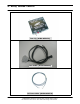
Exploded View and Parts List Discription SEC CODE BAG PE 6902-000297 CBF INTERFACE-MIC CABLE,BLK,S2 GH39-00727A CBF INTERFACE-DATA LINK CABLE( GH39-00859B ADAPTOR-ATADS10EBE,BLK,EU GH44-01702A S/W CD-SAMSUNG PC STUDIO 3.
6.
Main Electrical Parts List SEC CODE Design LOC Discription STATUS 1203-004416 U709 IC-DC/DC CONVERTER SA 1203-004518 U301 IC-BATTERY SA 1204-002746 U403 IC-TUNER SA 1205-002272 U203 IC-TRANSCEIVER SA 1205-002942 U103 IC-TRANSCEIVER SA 1205-003093 U102 IC-TRANSCEIVER SA 1205-003227 UCD401 IC-CODEC SA 1404-001165 TH301 THERMISTOR-NTC SA 1405-001082 V401 VARISTOR SA 1405-001082 V501 VARISTOR SA 1405-001108 VR608 VARISTOR SA 1405-001108 ZD601 VARISTOR SA 1405
Main Electrical Parts List SEC CODE Design LOC Discription STATUS 2007-000171 R305 R-CHIP SA 2007-000171 R426 R-CHIP SA 2007-000171 R427 R-CHIP SA 2007-000171 R701 R-CHIP SA 2007-000171 R706 R-CHIP SA 2007-000171 R713 R-CHIP SA 2007-000171 R720 R-CHIP SA 2007-000172 R708 R-CHIP SA 2007-001290 R226 R-CHIP SA 2007-001290 R227 R-CHIP SA 2007-001290 R515 R-CHIP SA 2007-001313 R410 R-CHIP SA 2007-007132 R304 R-CHIP SA 2007-007136 R309 R-CHIP SA 2007-00
Main Electrical Parts List SEC CODE Design LOC Discription STATUS 2007-008044 R616 R-CHIP SA 2007-008044 R617 R-CHIP SA 2007-008044 R618 R-CHIP SA 2007-008044 R633 R-CHIP SA 2007-008044 R634 R-CHIP SA 2007-008044 R635 R-CHIP SA 2007-008044 R636 R-CHIP SA 2007-008044 R637 R-CHIP SA 2007-008044 R638 R-CHIP SA 2007-008044 R639 R-CHIP SA 2007-008044 R640 R-CHIP SA 2007-008044 R641 R-CHIP SA 2007-008045 R217 R-CHIP SA 2007-008048 R111 R-CHIP SA 2007-00
Main Electrical Parts List SEC CODE Design LOC Discription STATUS 2007-008419 R510 R-CHIP SA 2007-008419 R511 R-CHIP SA 2007-008483 R307 R-CHIP SA 2007-008483 R319 R-CHIP SA 2007-008483 R513 R-CHIP SA 2007-008483 R619 R-CHIP SA 2007-008483 R620 R-CHIP SA 2007-008483 R705 R-CHIP SA 2007-008486 R721 R-CHIP SA 2007-008516 R108 R-CHIP SA 2007-008516 R113 R-CHIP SA 2007-008516 R212 R-CHIP SA 2007-008516 R213 R-CHIP SA 2007-008516 R317 R-CHIP SA 2007-00
Main Electrical Parts List SEC CODE Design LOC Discription STATUS 2007-008542 R425 R-CHIP SA 2007-008542 R428 R-CHIP SA 2007-008542 R429 R-CHIP SA 2007-008542 R430 R-CHIP SA 2007-008542 R431 R-CHIP SA 2007-008542 R433 R-CHIP SA 2007-008542 R434 R-CHIP SA 2007-008542 R517 R-CHIP SA 2007-008542 R524 R-CHIP SA 2007-008542 R535 R-CHIP SA 2007-008542 R536 R-CHIP SA 2007-008542 R537 R-CHIP SA 2007-008542 R539 R-CHIP SA 2007-008542 R545 R-CHIP SA 2007-00
Main Electrical Parts List SEC CODE Design LOC Discription STATUS 2007-008591 R521 R-CHIP SA 2007-008786 R230 R-CHIP SA 2007-008786 R306 R-CHIP SA 2007-008786 R522 R-CHIP SA 2007-008786 R523 R-CHIP SA 2007-008786 R552 R-CHIP SA 2007-008808 R204 R-CHIP SA 2007-008808 R205 R-CHIP SA 2007-008808 R206 R-CHIP SA 2007-008808 R207 R-CHIP SA 2007-008808 R208 R-CHIP SA 2007-008808 R209 R-CHIP SA 2007-008808 R210 R-CHIP SA 2007-008808 R211 R-CHIP SA 2007-00
Main Electrical Parts List SEC CODE Design LOC Discription STATUS 2203-000812 C409 C-CER,CHIP SA 2203-000812 C426 C-CER,CHIP SA 2203-000812 C427 C-CER,CHIP SA 2203-000812 C429 C-CER,CHIP SA 2203-000812 C430 C-CER,CHIP SA 2203-000995 U713 C-CER,CHIP SA 2203-001239 C525 C-CER,CHIP SA 2203-001239 C526 C-CER,CHIP SA 2203-001259 C101 C-CER,CHIP SA 2203-001259 C425 C-CER,CHIP SA 2203-002709 C216 C-CER,CHIP SA 2203-002709 C218 C-CER,CHIP SA 2203-002709 C227 C-
Main Electrical Parts List SEC CODE Design LOC Discription STATUS 2203-005682 C149 C-CER,CHIP SA 2203-005682 C601 C-CER,CHIP SA 2203-005682 C602 C-CER,CHIP SA 2203-005682 C603 C-CER,CHIP SA 2203-005682 C604 C-CER,CHIP SA 2203-005682 C605 C-CER,CHIP SA 2203-005682 C606 C-CER,CHIP SA 2203-005682 C607 C-CER,CHIP SA 2203-005682 C608 C-CER,CHIP SA 2203-005682 C611 C-CER,CHIP SA 2203-005682 C612 C-CER,CHIP SA 2203-005682 C613 C-CER,CHIP SA 2203-005682 C614 C-
Main Electrical Parts List SEC CODE Design LOC Discription STATUS 2203-005736 C122 C-CER,CHIP SA 2203-005736 C302 C-CER,CHIP SA 2203-005736 C306 C-CER,CHIP SA 2203-005736 C511 C-CER,CHIP SA 2203-005736 C621 C-CER,CHIP SA 2203-005806 C108 C-CER,CHIP SNA 2203-005806 C222 C-CER,CHIP SNA 2203-006048 C706 C-CER,CHIP SA 2203-006121 C145 C-CER,CHIP SA 2203-006121 C618 C-CER,CHIP SA 2203-006121 C701 C-CER,CHIP SA 2203-006121 C702 C-CER,CHIP SA 2203-006194 C105
Main Electrical Parts List SEC CODE Design LOC Discription STATUS 2203-006348 C722 C-CER,CHIP SA 2203-006423 C103 C-CER,CHIP SA 2203-006423 C104 C-CER,CHIP SA 2203-006423 C109 C-CER,CHIP SA 2203-006423 C135 C-CER,CHIP SA 2203-006423 C137 C-CER,CHIP SA 2203-006423 C139 C-CER,CHIP SA 2203-006423 C202 C-CER,CHIP SA 2203-006423 C203 C-CER,CHIP SA 2203-006423 C207 C-CER,CHIP SA 2203-006423 C208 C-CER,CHIP SA 2203-006423 C209 C-CER,CHIP SA 2203-006423 C210 C-
Main Electrical Parts List SEC CODE Design LOC Discription STATUS 2203-006423 C747 C-CER,CHIP SA 2203-006423 C748 C-CER,CHIP SA 2203-006466 C314 C-CER,CHIP SA 2203-006556 C113 C-CER,CHIP SA 2203-006562 C221 C-CER,CHIP SA 2203-006562 C226 C-CER,CHIP SA 2203-006562 C311 C-CER,CHIP SA 2203-006562 C313 C-CER,CHIP SA 2203-006562 C321 C-CER,CHIP SA 2203-006562 C402 C-CER,CHIP SA 2203-006562 C404 C-CER,CHIP SA 2203-006562 C414 C-CER,CHIP SA 2203-006562 C431 C-
Main Electrical Parts List SEC CODE Design LOC Discription STATUS 2203-006648 C110 C-CER,CHIP SA 2203-006648 C115 C-CER,CHIP SA 2203-006648 C503 C-CER,CHIP SA 2203-006668 C423 C-CER,CHIP SA 2203-006681 C623 C-CER,CHIP SA 2203-006824 C138 C-CER,CHIP SA 2203-006824 C312 C-CER,CHIP SA 2203-006825 C102 C-CER,CHIP SA 2203-006825 C323 C-CER,CHIP SA 2203-006825 C440 C-CER,CHIP SA 2203-006825 C703 C-CER,CHIP SA 2203-006825 C705 C-CER,CHIP SA 2203-006825 C731 C-
Main Electrical Parts List SEC CODE Design LOC Discription STATUS 2404-001381 C305 C-TA,CHIP SA 2404-001381 C415 C-TA,CHIP SA 2404-001381 C628 C-TA,CHIP SA 2404-001381 TA101 C-TA,CHIP SA 2404-001381 TA301 C-TA,CHIP SA 2404-001381 TA302 C-TA,CHIP SA 2404-001381 TA703 C-TA,CHIP SA 2404-001381 TA706 C-TA,CHIP SA 2404-001381 TA707 C-TA,CHIP SA 2404-001397 TA604 C-TA,CHIP SA 2404-001415 TA701 C-TA,CHIP SA 2404-001478 TA403 C-TA,CHIP SA 2404-001478 TA404 C-TA
Main Electrical Parts List SEC CODE Design LOC Discription STATUS 3301-001342 F602 BEAD-SMD SA 3301-001342 F603 BEAD-SMD SA 3301-001342 F604 BEAD-SMD SA 3301-001659 L110 BEAD-SMD SA 3301-001729 L401 BEAD-SMD SA 3301-001935 C432 BEAD-SMD SA 3404-001303 TAC601 SWITCH-TACT SA 3404-001303 TAC602 SWITCH-TACT SA 3408-001132 SW641 SWITCH-SLIDE SA 3705-001358 RFS101 CONNECTOR-COAXIAL SA 3709-001465 CN601 CONNECTOR-CARD EDGE SA 3710-002499 IFC501 SOCKET-INTERFACE S
7. Disassembly and Assembly Instructions 7-1. Disassembly 1 2 1) Be cautious not to damage the rear cover ※ caution 1. Remove a screw at six points as shown. ※ caution 1. Make space between rear cover and front cover from the lower part of set, by assembly stick. 3 4 1) Be cautious not to damage FPCB and connector ※ caution 1. Remove a hold key and a volume key as 1) Be cautious not to damage FPCB and connector ※ caution shown. 2. Separate the camera connector 1.
Exploded View and Parts List 6 5 1) when removing the screws from camera housing, be careful not to damage the housing ※ caution 1.Remove the screw at the left and right side of camera housing 2. Separate the camera housing from PBA. 3. Separate the PBA from the SET. ※ caution 1. Let it open by turning the front to the clockwise. 7 8 ※ caution ※ caution 1. After the front open, pull it down as shown. 1.Swing the hinge in the counter clockwise 2. The swing ASS'Y and the front separate by 2.
Exploded View and Parts List 10 9 ※ caution ※ caution 1. Loosen the screw at the five points of lower 1. By a assembly stick, separate the lower from case. the lower part. 11 12 ※ caution 1.Take out the vibration motor from the land. ※ caution 2.Remove the speaker. 1. Remove the sub-PCB from upper.
Exploded View and Parts List 13 14 1) When removing bracket, be cautious not to 1) When removing bracket , be cautious not to damage. damage FPCB. ※ caution ※ caution 1.Open the bracket by lifting to the left. 1. Lift the locker of connector. 2.Remove the green insulated tape. 2.Separate the wheel key ass'y. 15 16 ※ caution 1. Remove the bond. ※ caution 2. Separate the motor and speaker after lead is 1. Separate the main connector as shown. removed using soldering tool.
Exploded View and Parts List 7-2. Assembly 2 1 1) Insert by the shown guide line. ※ caution 1. Insert the wheel key ASS'Y according to guide line 2. Fix it by locker after inserting connector. 3. Put the tape on the locker to fix locker. ※ caution 1. Connect the MAIN FPCB on the LCD ASS'Y. 3 4 1) Remove tape 2) Check whether hole of bracket and hole of PCB are aligned. ※ caution 1. Remove the tape of the bracket. 2. Land wheel key ASS'Y according to PCB hole, folding sub-PCB.
Exploded View and Parts List 6 5 1) Push the lower after the lower and upper are combined. ※ caution 1.Let the main connector go through the hole of lower. ※ caution 1.Assemble upper and lower after hook of lower and locker of lower are combined. 7 8 1) Be cautious not to damage cover sticker. ※ caution 1.Fasten the 5 point screws at the lower. ※ caution 1.Put the cover sticker at the five point of the lower.
Exploded View and Parts List 10 9 ※ caution ※ caution 1. According to the hinge shape, combine the front 1. Align the front and the lower by means of upper part as shown. swinging to the counter clock wise. 11 12 check the MIC as shown. Check the position of MIC, again. caution Land the MIC on the desired position, exactly Turning PBA up to 90 degree, insert FPCB into the hole. 3. Land PBA as shown. 1) Align the hole of housing and the hole of PBA.
Exploded View and Parts List 14 13 1) ※ 1. 2. Check the position of +/caution Combine the volume key. Combine the hold key. 15 ※ caution 1.Check the status of each connector, volume key,and hold key. 16 1) Push rear carefully when assembling rear ※ caution 1. Combine the hook of rear's upper on the locker of front. 2. Combine sequentially from up and down. ※ caution 1. Fasten screws at the 6 point of the rear.
Exploded View and Parts List 7-3. Wheel key Assembly 2 1 1)Check the whether a magnetic is in bracket. ※ caution 1. Attach the deco on the wheel key 1)Wheel key can not be on the rib of the bracket. ※ caution 1.Land the wheel key to the direction, where rib 2. Remove the tape on the top of bracket does not exist.
8.
Block Diagrams 8-2 SAMSUNG Proprietary-Contents may change without notice This Document can not be used without Samsung's authorization
9.
PCB Diagrams JTAG201 U706 F105 TP502TP501 TP206TP205 U302 CPU201 TH301 OSC501 OSC201 TA701 U701 SW641 TA302 CPU501 TA502 TP512 TP503TP209 D701 VR604 TAC601 VR607 TA501 TP504 TA301 TP510 U301 TP511 U707 TP509 TA504 TP508 TP505 TA703 TP507 TP506 U103 U704 VR605 V601 U601 OSC102 U401 T AC602 U713U711 F603 USB_DUSB_D+_J VBAT_JSDS_TXD_J SDS_RXD_J USB_201GND_J JIG_ON_J CPU301 TP301 UME201 TP204 TP207 UME202 U402 TA404 TA403 TA402 UCD401 F401 TP203TP208 9-2 S
10. Chart of Troubleshooting 10-1.Baseband 10-1-1. Power ON 'Power On' dose not work YES Check the current consumption more than 100mA NO Download again Check R642, VR608 NO Change the Battery or Recharging the battery YES Check the Vbat more than 3.3V YES Check the HP_CORE_1.57V ≥ 1.57 and HPEIO_1.8V≥ 1.8V NO Check U701 and C703 and C705 YES Check VCCD_2.8V and VRST_1.8V of CPU301 NO Check CPU301, C308 and C307 YES Check VRF_2.9V and VCCB_2.
Flow Chart of Troubleshooting and Circuit Diagrams 10-2 SAMSUNG Proprietary-Contents may change without notice This Document can not be used without Samsung's authorization
10.
Flow Chart of Troubleshooting and Circuit Diagrams 10-4 SAMSUNG Proprietary-Contents may change without notice This Document can not be used without Samsung's authorization
SERLE SERDAT SERCLK RF_EN TX_EN VBS1 VBS2 MODE_SEL XOENA DSP_IO DSP_RWN FLASH_RESET R305 10-5 SAMSUNG Proprietary-Contents may change without notice This Document can not be used without Samsung's authorization AOUTAP AOUTAN AOUTBP AOUTBN MICINP MICINN MICOUTP MICOUTN AUXINP AUXINN AUXOUTP AUXOUTN RTXIP RTXIN RTXQP RTXQN AFC VAPC OCTL0 OCTL1 OCTL2 OCTL3 OCTL4 OCTL5 OCTL6 OCTL7 SERLE1 SERLE2 SERDA SERCK E6 C5 F5 E5 A4 G6 B3 A3 B1 A2 C1 C2 C320 AFC TXP D9 E7 DSP_AB(0:8) DB15 DB14 DB13 DB12 DB
Flow Chart of Troubleshooting and Circuit Diagrams VBAT HP_CORE_1.57V VRST_1.8V HPEIO_1.8V U701 C701 L701 TA701 C703 C702 1 VFB1 VFB2 10 2 VOUT OUT2 9 3 VIN RUN1 8 4 SW1 SW2 7 5 GND 6 RUN2 GND 11 VCCD_2.8 D701 R702 L702 C706 C705 VRF_2.9V_REG VPC R104 C107 C150 VAPC VRF_2.9V C108 VCCD_2.
Flow Chart of Troubleshooting and Circuit Diagrams 10-1-2. System Initial Initial Failure YES Check the VCCD_2.8V of CPU301 is "High" When the phon e is boot on NO Check CPU301 YES check the VCCD_2.8 of U701 is "High" NO Check U701 YES Voltage at the R702 is NO Check CPU301 and R702 "Low-> High"? YES There is 32.768KHz wave NO Check OSC201 form at the C223, C224 ? YES LCD display is O.K? NO Check HDC601 and LCD part YES Sound is O.
Flow Chart of Troubleshooting and Circuit Diagrams 10-8 SAMSUNG Proprietary-Contents may change without notice This Document can not be used without Samsung's authorization
Flow Chart of Troubleshooting and Circuit Diagrams 10-9 SAMSUNG Proprietary-Contents may change without notice This Document can not be used without Samsung's authorization
Flow Chart of Troubleshooting and Circuit Diagrams 10-1-3. Sim Part "Insert SIM" is displayed on the LCD Check the SIM connector's NO (CN601)connection to SIM card? Resolder or change CN601 or connect again YES NO Check the voltage at Pin #11 of CN601 >=2.
Flow Chart of Troubleshooting and Circuit Diagrams 10-11 SAMSUNG Proprietary-Contents may change without notice This Document can not be used without Samsung's authorization
Flow Chart of Troubleshooting and Circuit Diagrams 10-1-4.
Flow Chart of Troubleshooting and Circuit Diagrams 10-13 SAMSUNG Proprietary-Contents may change without notice This Document can not be used without Samsung's authorization
Flow Chart of Troubleshooting and Circuit Diagrams 10-1-5. Microphone Part Microphone does not work YES Check the assembled status of microphone NO Reassemble microphone YES Check the soldering status of KeyFPCB NO Change KeyFPCB YES Check the reference voltage on mic path R410=2.8V NO Resolder or Change (C309, R415, R414,V402,C426,C417, V401,C410,R412,TA407,TA406,R410) YES Is Microphone O.
Flow Chart of Troubleshooting and Circuit Diagrams 10-15 SAMSUNG Proprietary-Contents may change without notice This Document can not be used without Samsung's authorization
Flow Chart of Troubleshooting and Circuit Diagrams MAIN MIC R401 AUXOUTP C401 EAR_MIC_P EAR_MIC_N C403 R404 C405 R406 AUXINP AUXINN R407 VCCA_2.
Flow Chart of Troubleshooting and Circuit Diagrams 10-1-6. Receiver Part Speaker dose not work YES Check the LCD module connection NO Reassemble LCD Module YES Check the R220 ="Low" NO Resolder R220 YES Check the R418 & R419 NO Resolder R418, R419 YES Check the ZD601, ZD602 NO Change U401 YES Is Speaker O.
Flow Chart of Troubleshooting and Circuit Diagrams 10-1-7. Speaker Part Speaker dose not work YES Check the LCD module connection NO Reassemble LCD Module YES Check the R220 ="High" NO Resolder R220 YES Check the R426,R427 ="PWM Wave" NO Change the L401 YES Check the ZD601, ZD602 NO Change U401 YES Is Speaker O.
Flow Chart of Troubleshooting and Circuit Diagrams 10-19 SAMSUNG Proprietary-Contents may change without notice This Document can not be used without Samsung's authorization
Flow Chart of Troubleshooting and Circuit Diagrams 10-1-9. LCD Camera function dose not work YES First, Check the Connection of HDC601 and LCD YES Have a some problem of Cable (FPCB) YES Replace the cable(FPCB) No Display is not NO Check the MV_2.
Flow Chart of Troubleshooting and Circuit Diagrams 10-21 SAMSUNG Proprietary-Contents may change without notice This Document can not be used without Samsung's authorization
11. Reference data 11-1. Reference Abbreviate AAC: Advanced Audio Coding. AVC : Advanced Video Coding.