COLOR TELEVISION RECEIVER Chassis : Model : COLOR TELEVISION RECEIVER KS2A(N) (REV.2) CFT24907X/SMS CONTENTS 1. Precautions 2. Reference Information 3. Specifications 4. Alignment and Adjustments 5. Troubleshooting 6. Exploded Views and Parts List 7. Electrical Parts List 8. Block Diagrams 9. Wiring Diagram 10.
ELECTRONICS © Samsung Electronics Co., Ltd. MAY.
Precautions 1. Precautions Follow these safety, servicing and ESD precautions to prevent damage and protect against potential hazards such as electrical shock and X-rays. 1-1 Safety Precautions 1. Be sure that all of the built-in protective devices are replaced. Restore any missing protective shields. 2. When reinstalling the chassis and its assemblies, be sure to restore all protective devices, including: nonmetallic control knobs and compartment covers. 3.
Precautions 1-1 Safety Precautions (Continued) 9. High voltage is maintained within specified limits by close-tolerance, safety-related components and adjustments. If the high voltage exceeds the specified limits, check each of the special components. 10. Design Alteration Warning: Never alter or add to the mechanical or electrical design of this unit. Example: Do not add auxiliary audio or video connectors. Such alterations might create a safety hazard.
Precautions 1-2 Servicing Precautions Warning1: First read the “Safety Precautions” section of this manual. If some unforeseen circumstance creates a conflict between the servicing and safety precautions, always follow the safety precautions. Warning2: An electrolytic capacitor installed with the wrong polarity might explode. 1. Servicing precautions are printed on the cabinet. Follow them. 2.
Precautions 1-3 Precautions for Electrostatically Sensitive Devices (ESDs) 1. Some semiconductor (“solid state”) devices are easily damaged by static electricity. Such components are called Electrostatically Sensitive Devices (ESDs); examples include integrated circuits and some field-effect transistors. The following techniques will reduce the occurrence of component damage caused by static electricity. 2.
Reference Information 2.
Reference Information Table 2-2 Table of Acronyms ABL AC ACC AF AFC AFT AGC AM ANSI APC APC A/V AVC BAL BPF B-Y CATV CB CCD CCTV Ch CRT CW DC DVM EIA ESD ESD FBP FBT FF FM FS GND G-Y H HF HI-FI IC IC IF 2-2 Automatic Brightness Limiter Alternating Current Automatic Chroma Control Audio Frequency Automatic Frequency Control Automatic Fine Tuning Automatic Gain Control Amplitude Modulation American National Standards Institute Automatic Phase Control Automatic Picture Control Audio-Video Automatic Volume C
Reference Information 2-2 IC Line Up Table 2 - 3 IC Line - Up NO 1 BOARD MAIN LOC.
Reference Information Table 2-3-1 VIDEO IC SPEC VDP3108B Basic 1H Comb Filter VDP3130Y 2H Comb Filter, DVD Input FUNCTION REMARK FUNCTION REMARK Table 2-3-2 SOUND AMP SPEC TDA7297 2-4 7W x 2CH, 10W x 2CH Samsung Electronics
Specifications 3. Specifications Television System Multi Antena Input Consumption Power Requirements Frequency NTSC-M, PAL N.
MEMO 3-2 Samsung Electronics
Alignment and Adjustments 4. Alignment and Adjustments 4-1 General Alignment Instructions 1. Usually, a color TV-VCR needs only slight touch-up adjustment upon installation. Check the basic characteristics such as height, horizontal and vertical sync and focus. 5. Avoid overload. Excessive signal from a sweep generator might overload the front-end of the TV. When inserting signal markers, do not allow the marker generator to distort test results. 2. Observe the picture for good black and white details.
Alignment and Adjustments 4-4 FOCUS Adjustment 1. Input a black and white signal. 2. Adjust the tuning control for the clearest picture. 3. Adjust the FOCUS control for well defined scanning lines in the center area of the screen. 4-5 SCREEN Adjustment 1. Input Toshiba Pattern 2. Enter “Service Mode”.(Refer to “4-8-1 Service Mode”) 3. Select “G2-Adjust”. 4. Set the values as below. Table 1.
Alignment and Adjustments 4-6 E2PROM (IC902) Replacement 1. When IC902 is replaced, all adjustment data revert to the initial values. So, all adjustment values when servicing should be readjusted. 2. After IC902 is replaced, connect the AC power supply cord. 3. Turn the power switch ON. 4. In stand-by, warm up the TV for at least 10 seconds. 5. Power on the TV. 4-7 White Balance Adjustment Equipment : Color-Analyzer (CA-100) Input Signal : Pattern signal (Toshiba pattern) 1. Select STANDARD from the menu.
Alignment and Adjustments 4-8 Factory Adjustment 4-8-1 Service Mode 1. To enter the “Service Mode”, Press the remote-control keys in this sequence : - If you do not have Factory remote-control PICTURE OFF MUTE 1,8,2 PICTURE ON - If you have Factory remote-control PICTURE ON DISPLAY ( ) FACTORY 2. After the Service Mode is entered, the initial screen is as shown in the figure below. These hexa digits are check sum value which * depends on the MICOM version.
Alignment and Adjustments 4-8-2 Deflection (Memory Data) - SIM408A USA, LATIN FACTORY (VDP IC VDP3108B) 4-8-2(A) GEOMETRIC ADJUSTMENT VALUE INCH 27V 1.3R Model DEFLECTION H Bow H Angle H Dscc V SHIFT V AMP V SLOPE V SC H EW H TRAPEZIUM H PARABOLA H SYMMETRY H CORNER H SHIFT PIP CONTRAST PIP TINT PIP PAL V.POS PIP NTSC V.POS PIP H.
Alignment and Adjustments 4-8-2(B) SCREEN CHANGE (I2C BUS GEOMETRIC ADJUSTMENT) 1 V Shift 6 V Amp 2 V Slope 7 V SC 3 H EW 8 H Trapizium 4 H Parabola 9 H Symmetry 5 H Corner 10 H Shift 4-6 Samsung Electronics
H PARABOLA H SYMMETRY H CORNER H SHIFT PIP CONTRAST PIP TINT PIP PAL V.POS PIP NTSC V.POS PIP H.POS -13 13 15 4 Control FIX Control Control FIX FIX FIX FIX FIX 4-8-2(C) VIDEO ADJUST 1 INCH Model VIDEO ADJUST1 RED CUT OFF GREEN CUT OFF BLUE CUT OFF RED DRIVE GREEN DRIVE BLUE DRIVE SUB BRIGHT SUB CONTRAST SUB COLOR SUB TINT BCL THRESHOLD BCLGAIN BCL TIME DVD SUB TINT N.
8 13 90 0 BCLGAIN BCL TIME DVD SUB TINT N. YC DELAY FIX FIX FIX FIX 8 10 100 3 8 10 100 3 8 10 100 3 27V 1.3R 23V 1.
TXK2566 TXK2754 TXK2567 CL663BW VIDEO ADJUST3 INIT PEAK WHITE LIMLT 255 FIX 255 255 SOFT LIMIT SLOPE B 4 FIX 4 4 HARD LIMIT 255 FIX 255 255 INCH 27V 1.3R 23V 1.3R MODULATION ON/OFF 0 FIX 0 0 A TILT POINT 0 FIX 0 0 Model CL25D4W Note 2.
Alignment and Adjustments 4-8-3 Deflection (Memory Data) - SIM408A USA, LATIN FACTORY (VDP IC VDP3130Y) 4-8-3(A) GEOMETRIC ADJUSTMENT VALUE INCH 27V 1.3R Model DEFLECTION H Bow H Angle H Dscc V SHIFT V AMP V SLOPE V SC H EW H TRAPEZIUM H PARABOLA H SYMMETRY H CORNER H SHIFT PIP CONTRAST PIP TINT PIP PAL V.POS PIP NTSC V.POS PIP H.POS 4-10 INIT 0 0 0 -40 5 -2 -7 64 -20 -13 13 15 4 FIX FIX FIX Control Control Control FIX Control Control Control FIX Control Control FIX FIX FIX FIX FIX 23V 1.
Alignment and Adjustments 4-9 MICOM 4-9-1 Pin Layout Write Protect EEPROM SDA 1 I/O 2 I/O EEPROM SCL Bus-Stop Main SDA 3 IO I/O 50 4 I/O I/O 49 5 I/O 48 Main SCL Sound Reset Video Reset VDD 2.5V GND VDD 3.3V CVBS Input VDD 2.5V GND AFT Scart1 Ident Scart2 Ident Key 1 H-Sync V-Sync 6 I/O 47 7 I/O 46 8 I/O 45 9 10 11 12 13 14 15 ADC 16 ADC PWM 52 Tilt 51 N.C. Power Sound Mute N.C. N.C.
Alignment and Adjustments 4-9-2 Pin Assignment Specification PIN NO FUNCTION ASSIGN IN/OUT ACTIVE H/L Out Low DESCRIPTION 1 I/O Write Protect 2 I/O ROM SDA I/O EEPROM Serial Data Line 3 I/O ROM SCL I/O EEPROM Serial Clock Line 4 I/O Bus Stop In 5 I/O Main SDA I/O 6 I/O Main SCL I/O Low Peripheral IC Serial Clock Line 7 I/O Sound Reset Out Low MSP IC Initial Control 8 I/O Video Reset Out VDP IC Initial Control 9 Vdd VDD 2.5V 10 GND 11 Vdd VDD 3.
Alignment and Adjustments 4-9-2 Pin Assignment Specification (Continued) PIN NO FUNCTION ASSIGN IN/OUT ACTIVE H/L Out Low DESCRIPTION 27 I/O 28 N.C. Not Used (Programmed Gound Level) 29 GND Analog Ground 30 Vdd 31 N.C. Not Used (Programmed Gound Level) 32 N.C. Micom Hardware Reset 33 Reset Reset In Low Crystal Oscillation Input 34 X-In X-TAL In In 6MHz Crystal Oscillation Output 35 X-Out X-TAL Out Out 6MHz Analog Ground 36 GND 37 Vdd VDD 2.
MEMO 4-14 Samsung Electronics
Troubleshooting 5.
Troubleshooting 5-2 No Raster (Sound OK) No Raster (Sound OK) Check Fusible Resistance Check the fusible resistance of abnormal volatge line Abnormal Abnormal Check voltage of heater Normal Check Abnormal RK,GK,BK Signal output from CRT PCB Normal Abnormal Check CRT and FBT Abnormal Check the signal output from IC201 Pin 63 Normal Check / Replace IC201 5-2 Check R.G.B Signal input to CRT PCB Abnormal Check tuner B+ and Main CVBS Check R.G.
Troubleshooting 5-3 No Sound No Sound Normal Check Speaker and Wire Normal Check the signal output from 602 Pins Abnormal Abnormal Check the signal input to IC602 pins 4 ,12 Normal Check the signal input to IC601 Pin 47 Check IC602 B+ Abnormal Abnormal Normal Check IC601 B+ Check tuner B+ and SIF Check/Replace the resistance of FD802 Normal Replace IC602 Abnormal Check/Replace IC601 Samsung Electronics Check B+ Line (8V) 5-3
Troubleshooting 5-4 Horizontal Lines Appear on screen Horizontal Lines Apper on screen Normal Normal Check the VDP Signal output from IC201 Pin 31 Check IC301 B+ (16V, -16V) Abnormal Check B+ Line and the fusible resistance of R425, 424 Abnormal Check/Replace IC301 5-4 Check IC201 Samsung Electronics
Exploded View & Parts List 6. Exploded View & Parts List 6-1 CFT24907X/SMS No Samsung Electronics Code No Description;Specification Q’ty Remark 1 AA64-02885A CABINET-FRONT;KS2A,25A6,MOLD,SAM’S 1 F/C 1-1 AA64-02886A DOOR-A/V;KS2A,25A6,ABS,HB,SAM’S 1 DOOR 1-2 AA64-02915A INLAY-A/V;PS,SHEET,T0.3 GRAY,25A6 1 IN/AV 1-3 AA64-02286A BADGE-BRAND;AKAI,AL FORGING,-,-,L65,-,SI 1 BADGE 1-4 AA61-00343A SPRING-CS;-,SUS304,-,-,-,-,0.
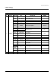
Electrical Parts List 7. Electrical Parts List 7-1 CFT27907X/SMS Loc. No. Code No. Description ; Specification Remark ASSY-CHASSIS 1 A/CHAS AA91-04171A ASSY-CHASSIS;KS2A,25,SINGLE V.
Electrical Parts List Loc. No.
Electrical Parts List Loc. No.
Electrical Parts List Loc. No.
Electrical Parts List Loc. No.
Electrical Parts List Loc. No.
Electrical Parts List Loc. No.
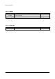
Electrical Parts List Loc. No. Code No. Description ; Specification Remark Loc. No. Code No. Description ; Specification ASSY-COVER/REAR 1 A/REAR AA90-03216A ASSY-COVER/REAR;25A6,HIPS,V0,G4309,KS2A, 2 2 2 2 2 2 2 CB+CF TER+RK SPCBC B/C AC+BC H/T INL/CA 6003-001026 6003-001026 AA63-60001X AA64-02882A AA65-30008A AA61-00356B AA64-02053A SCREW-TAPTITE;RH,+,B,M4,L15,ZPC(BLK),SWR SCREW-TAPTITE;RH,+,B,M4,L15,ZPC(BLK),SWR SPACER-FELT;FELT,T0.
Schematic Diagrams 8.
Schematic Diagrams 8-2 Block Diagram 8-2 Samsung Electronics
Wiring Diagram 9.
MEMO 9-2 Samsung Electronics
Schematic Diagrams 10.
Schematic Diagrams 10-2 MAIN 2/4 TP10 TP11 TP11 TP12 TP12 TP13 TP14 TP10 TP13 TP14 : Power Line : Signal Line 10-2 Samsung Electronics
Schematic Diagrams 10-3 MAIN 3/4 TP21 TP15 TP22 TP16 TP23 TP17 TP24 TP18 TP22 TP15 TP17 TP21 TP16 TP20 TP19 TP18 TP19 TP23 TP24 TP20 : Power Line : Signal Line Samsung Electronics 10-3
Schematic Diagrams 10-4 MAIN 4/4 TP31 TP25 TP32 TP26 TP33 TP27 TP34 TP28 TP32 TP25 TP26 TP31 TP33 TP27 TP30 TP28 TP29 TP29 TP30 : Power Line : Signal Line 10-4 Samsung Electronics