GSM TELEPHONE SGH-E870 GSM TELEPHONE CONTENTS 1. Safety Precautions 2. Specification 3. Product Function 4. Array course control 5. Exploded View and Parts List 6. Disassembly and Assembly instructions 7. MAIN Electrical Parts List 8. Block Diagrams 9. PCB Diagrams 10. Flow Chart of Troubleshooting 11.
Contents 1. Safety Precautions 1-1. Repair Precaution ...........................................................................1-1 1-2. ESD(Electrostatically Sensitive Devices) Precaution ...........................1-2 2. Specification 2-1. GSM General Specification ..............................................................2-1 2-2. GMSK TX Power Level ....................................................................2-2 2-3. EDGE TX Power Level .......................................................
Contents 10-1-2. 10-1-3. 10-1-4. 10-1-5. 10-1-6. 10-1-7. 10-2. RF 10-2-1. 10-2-2. 10-2-3. 10-2-4. 10-2-5. Initial ....................................................................................10-4 Sim Part ...............................................................................10-6 Microphone Part .....................................................................10-8 Speaker Part ........................................................................10-10 Camera Part ......................
1. Safety Precautions 1-1. Repair Precaution ● Repair in Shield Box, during detailed tuning. Take specially care of tuning or test, because specipicty of cellular phone is sensitive for surrounding interference(RF noise). ● Be careful to use a kind of magnetic object or tool, because performance of parts is damaged by the influence of manetic force. ● Surely use a standard screwdriver when you disassemble this product, otherwise screw will be worn away. ● Use a thicken twisted wire when you measure level.
Safety Precautions 1-2. ESD(Electrostatically Sensitive Devices) Precaution Several semiconductor may be damaged easilly by static electricity. Such parts are called by ESD(Electrostatically Sensitive Devices), for example IC,BGA chip etc. Read Precaution below. You can prevent from ESD damage by static electricity. ● Remove static electricity remained your body before you touch semiconductor or parts with semiconductor.
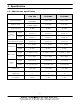
2. Specification 2-1. GSM General Specification GSM 900 DCS1800 PCS1900 F r e q . Ba n d [ M Hz ] Uplink/ Downlink 88 0~9 15 92 5~9 60 1710~1785 1805~1880 1850~1910 1930~1990 AR FC N range 0~12 4 & 9 75 ~10 23 512~885 512~810 T x /Rx s pacing 45 M Hz 95 M Hz 80 M Hz G P RS 270.833 Kbp s 3.692 us 270.833 Kbp s 3.692 us 270.833 Kbp s 3.692 us EDGE 812.5 K bp s 3.692 us 812.5 K bp s 3.692 us 812.5 K bp s 3.692 us 576.9 u s 4.615 ms 576.9 u s 4.615 ms 576.9 u s 4.615 ms G P RS 0.
Specification 2-2.
Specification 2-3.
3. Product Function Main Function -Camera and camcorder Use the camera module on your phone to take a photo or record a video. -Music player Play music files using your phone as a music player. -Web browser Access the wireless web to get up-to-the-minute information and a wide variety of media content. -Image editor Crop, resize, rotate, and decorate your photos. -Voice commands Experience a new level of voice command capability that allows for easy hands-free use.
4.
Array course control Software Downloading 4-1. Downloading Binary Files • Two binary files for downloading E870. – E870XXYY.s3 : Main source code binary. – E870XXYY.cts : Default Contents binary. 4-2. Pre-requsite for Downloading • Downloader Program(OptiFlash.
Array course control 4-3. S/W Downloader Program 1. Load the binary download program by executing the “OptiFlash.exe” 2. Select the “Options” -> “Settings” -> “Generic” -> “Specify hardware platform”. Choose hardware platform for the downloader file setting.
Array course control 3. Select the COM port when the download cable is connected Up to 64 ports are supported. Additionally you can select the maximum transfer speed OptiFlash will use to communicate with the phone.
Array course control 4. Select the“Flash&Verify” -> “Browse” Set the directory path and choose the latest s/w binary, for example “E870XXYY.s3”, for the downloader binary setting. In case of E870 the reserved regions are not a necessity. (It is defined in platform.
Array course control 5. Select the“Default Contents” -> “Browse” Set the directory path and choose the CTS file, for example “E870XXYY.cts”, for the downloader binary setting.
Array course control 6. Click “OK” button then press “Flash”. (Before pressing ‘Flash’ button, push the button ‘*’and ‘END’ at the same time. Then press ‘Flash’.) Downloader will upload the binary file as below for the downloading. 7. When downloading is finished successfully, there is a “All is well” message. 8. After finishing downloading, Certain memory resets should be done to guarantee the normal performance. 9. Confirm the downloaded version name and etc.
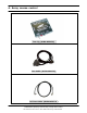
5. Exploded View and Parts List 5-1.
Exploded View and Parts List 5-2.
Exploded View and Parts List Discription SEC CODE BAG PE 6902-000297 CBF INTERFACE-DATA LINK CABLE GH39-00444B ADAPTOR-SGHD800 TA(EU) GH44-01060B S/W CD-SAMSUNG PC STUDIO GH46-00225A UNIT-EARPHONE GH59-02499B LABEL(P)-WATER SOAK GH68-02026A LABEL(P)-WATER SOAK GH68-02026A MANUAL-WARRANTY CARD GH68-02623A MANUAL-SFC GH68-04336A LABEL(P)-BARCODE RUSSIA GH68-08494A LABEL(R)-MAIN (SER) GH68-09068B MANUAL USERS-EU RUSSIAN GH68-09119A CUSHION-CASE TA2 MA2 GH69-03580A BOX(P)-UNIT MAIN
6. Disassembly and Assembly instructions 6-1. Assembly 1 2 WIRE arrangement CAMERA SAFE ARRIVAL POSITION SPEAK CENTER GASKET LCD FPCB GASKET 1. Insert LCD F-PCB at FOLDER LOWER. 2. Safe arrival in turn CAMERA / FLASH BRACKET. 3. Attach in turn SPEAK CENTER GASKET or LCD FPCB GASKET at LCD(SUB LCD). ※ caution 1. When safe arrival the FLASH BRACKET, Take care. 2. Perfectly safe arrival CAMERA or FLASH BRACKET. insulated TAPE 1. Safe arrival in turn MOTOR / SPEAK. 2.
Disassembly and Assembly instructions 5 6 ② ① Insert to LCD FPCB ③ SIM FPCB Insert HINGE 1. Put the PBA. 2. Assemble LCD CONNECTOR. ※ caution 1. 2. 3. 4. SIM BRACKET Assemble the SIM CONNECTOR. Put the SIM BRACKET. Remove the paper at SIM BRACKET. Assemble SIM FPCB at SIM BRACKET. ※ caution 1. Connect SIM CONNECTOR perfectly. 2. Fix into HOLE, when put the SIM BRACKET. 3. Check to come off the SIM FPCB at SIM BRACKET. 1. Do not damage to put the PBA. 2. Connect LCD CONNECTOR perfectly. 3.
Disassembly and Assembly instructions 6-2. Disassembly 1 2 Diassembly FOLLDER SIM ASSAY ANT CONTACT SIM CONNECTOR SIM BRACKET fixed SCREW 1. Loose the fixed screw at sim braket. 2. Separate the sim Assay at B'D. 1. Loose the four screws at the rear cover. 3. Disconnect the LCD connector at B'D. 2. Open the rear cover from bottom-side hook. ※ caution ※ caution 1. Do not scratch at rear cover & front. 2. Do not come off SIM BRACKET EMI metalization. 1. Handle with care SIM F-PCB & LCD F-PCB.
Disassembly and Assembly instructions 5 6 CAMERA 3 1 5 2 4 1 2 1. In turn MOTOR/SPEAKER/CAMERA/FLASH 1. Open a groove of FOLDER UPPER of the right top portion by JIG, separating folder upper. ※ caution BRACKET/ LCD F-PCB, separate to folder lower. 1. Do not scratch at folder upper & lower. 2. Seperate the LCD at folder lower. ※ caution 2. Handle the hook of FOLDER UPPER / LOWER 1. Do not damage when removed CAMERA or with care. FLASH BRACKET. 2. Take care of LCD F-PCB.
Disassembly and Assembly instructions 6-3. KIT Assembly 2 1 SPEAK RUBBER LCD CENTER RUBBER 1. Check the LCD MODULE apperance condition. 2. Check the LCD CONNECTOR condition. SUB LCD RUBBER A SUB LCD RUBBER B 1. Attach to SPEAK RUBBER / LCD CENTER RUBBER. 2. Attach to SUB LCD RUBBER A / B. ※ caution 1. Do not touch front side of LCD (fingerprint) 2. Do not scratch LCD F-PCB by tweezers when attach the PORON. ※ caution 1. Do not touch front side of the LCD. (fingerprint) 3 1.
7.
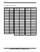
Main Electrical Parts List SEC CODE Design LOC Discription 2203-000254 C141 C-CER,CHIP SA 2203-006048 C142 C-CER,CHIP SA 2203-006562 C143 C-CER,CHIP SA 2203-000311 C144 C-CER,CHIP SA 2203-006048 C145 C-CER,CHIP SA 2203-006562 C148 C-CER,CHIP SA 2203-006562 C149 C-CER,CHIP SA 2203-006194 C152 C-CER,CHIP SA 2203-006194 C201 C-CER,CHIP SA 2203-006194 C202 C-CER,CHIP SA 2203-006423 C203 C-CER,CHIP SA 2203-006423 C204 C-CER,CHIP SA 2203-006423 C205 C-CER,CHIP
Main Electrical Parts List SEC CODE Design LOC Discription 2203-006562 C314 C-CER,CHIP SA 2203-006562 C315 C-CER,CHIP SA 2203-006562 C316 C-CER,CHIP SA 2203-006562 C317 C-CER,CHIP SA 2203-006562 C318 C-CER,CHIP SA 2203-006562 C319 C-CER,CHIP SA 2203-000233 C320 C-CER,CHIP SA 2203-005344 C321 C-CER,CHIP SA 2203-001405 C322 C-CER,CHIP SA 2203-000254 C323 C-CER,CHIP SA 2203-006257 C324 C-CER,CHIP SA 2203-006562 C325 C-CER,CHIP SA 2203-002709 C326 C-CER,CHIP
Main Electrical Parts List SEC CODE Design LOC Discription 2203-002982 C414 C-CER,CHIP SNA 2203-002982 C415 C-CER,CHIP SNA 2203-000854 C417 C-CER,CHIP SA 2203-006324 C418 C-CER,CHIP SA 2203-006562 C419 C-CER,CHIP SA 2203-000278 C420 C-CER,CHIP SA 2203-000278 C421 C-CER,CHIP SA 2404-001352 C422 C-TA,CHIP SA 2203-006257 C423 C-CER,CHIP SA 2203-006562 C424 C-CER,CHIP SA 2203-002709 C425 C-CER,CHIP SNA 2203-002709 C426 C-CER,CHIP SNA 2203-006626 C427 C-CER,C
Main Electrical Parts List SEC CODE Design LOC Discription 2203-006423 C453 C-CER,CHIP SA 2203-006423 C454 C-CER,CHIP SA 2203-006379 C455 C-CER,CHIP SA 2203-005682 C456 C-CER,CHIP SA 2203-006562 C457 C-CER,CHIP SA 2203-006048 C458 C-CER,CHIP SA 2404-001381 C501 C-TA,CHIP SA 2203-006257 C502 C-CER,CHIP SA 2203-006423 C518 C-CER,CHIP SA 2203-006423 C519 C-CER,CHIP SA 2203-006562 C520 C-CER,CHIP SA 2203-006562 C521 C-CER,CHIP SA 2203-000254 C522 C-CER,CHIP
Main Electrical Parts List SEC CODE Design LOC Discription 3705-001358 CN101 CONNECTOR-COAXIAL SA 3711-005550 CN302 HEADER-BOARD TO BOARD SA 3711-006138 CN504 HEADER-BATTERY SA 3710-002306 CN506 SOCKET-INTERFACE SA 3708-001956 CN507 CONNECTOR-FPC/FFC/PIC SA 3301-001342 F201 BEAD-SMD SA 2901-001256 F301 FILTER-EMI SMD SA 2901-001320 F501 FILTER-EMI/ESD SA 2901-001320 F502 FILTER-EMI/ESD SA 2901-001320 F503 FILTER-EMI/ESD SA 2901-001320 F504 FILTER-EMI/ESD SA 29
Main Electrical Parts List SEC CODE Design LOC Discription 2007-008049 R106 R-CHIP SA 2007-008587 R107 R-CHIP SA 2007-008045 R108 R-CHIP SA 2007-009223 R109 R-CHIP SA 2007-000138 R110 R-CHIP SA 2007-007095 R111 R-CHIP SA 2007-007134 R112 R-CHIP SA 2007-009199 R113 R-CHIP SA 2007-008483 R114 R-CHIP SA 2007-007142 R115 R-CHIP SA 2007-000171 R116 R-CHIP SA 2007-000157 R117 R-CHIP SA 2007-000171 R118 R-CHIP SA 2007-009111 R119 R-CHIP SA 2007-008516 R2
Main Electrical Parts List SEC CODE Design LOC Discription 2007-000171 R404 R-CHIP SA 2007-008672 R405 R-CHIP SA 2007-007311 R406 R-CHIP SA 2007-008542 R407 R-CHIP SA 2007-008542 R408 R-CHIP SA 2007-007311 R409 R-CHIP SA 2007-007311 R410 R-CHIP SA 2007-000171 R411 R-CHIP SA 2007-008672 R412 R-CHIP SA 2007-000170 R414 R-CHIP SA 2007-008544 R415 R-CHIP SA 2007-000152 R418 R-CHIP SA 2007-008478 R420 R-CHIP SA 2007-008478 R421 R-CHIP SA 2007-000141 R4
Main Electrical Parts List SEC CODE Design LOC Discription 2007-008483 R449 R-CHIP SA 2007-008420 R450 R-CHIP SA 2007-008542 R451 R-CHIP SA 2007-008542 R453 R-CHIP SA 2007-000142 R505 R-CHIP SNA 2007-000157 R506 R-CHIP SA 2007-000162 R507 R-CHIP SA 2007-008486 R509 R-CHIP SA 2007-008483 R510 R-CHIP SA 2007-008483 R511 R-CHIP SA 2007-008483 R512 R-CHIP SA 2007-008542 R513 R-CHIP SA 2007-008544 R514 R-CHIP SA 2007-001290 R515 R-CHIP SA 2007-001290 R
Main Electrical Parts List SEC CODE Design LOC Discription 2007-001339 R550 R-CHIP SA 2007-008786 R551 R-CHIP SA 3404-001152 SW1 SWITCH-TACT SA 3404-001152 SW2 SWITCH-TACT SA 3404-001152 SW3 SWITCH-TACT SA 1404-001165 TH301 THERMISTOR-NTC SA 2911-000021 U100 DUPLEXER-FEM SA 1001-001336 U102 IC-ANALOG SWITCH SA 4709-001374 U103 BLUETOOTH MODULE SA 1203-003432 U104 IC-POSI.FIXED REG.
Main Electrical Parts List SEC CODE Design LOC Discription 0801-002529 U507 IC-CMOS LOGIC SA 1201-002294 U508 IC-POWER AMP SA 1405-001082 V201 VARISTOR SA 1405-001082 V301 VARISTOR SA 1405-001082 V302 VARISTOR SA 1405-001082 V303 VARISTOR SA 1405-001082 V304 VARISTOR SA 1405-001082 V305 VARISTOR SA 1405-001082 V306 VARISTOR SA 1405-001082 V307 VARISTOR SA 1405-001082 V308 VARISTOR SA 1405-001082 V309 VARISTOR SA 1405-001082 V310 VARISTOR SA 1405-001082
8. Block Diagrams 8-1.
9.
U203 PCB Diagrams STO UP I RIGHT LEFT MENU PWR DOWN SEND CLEAR H_GPIO9 2 5 6 8 9 3 1 4 7 H_GPIO8 T_NINT T_OCS T_A(1) T_D(1) T_OEN TP201 SHARP * 0 TP301 TP302 DAICK DAIDO DAIDI V400 T_DSP_IO V306 V307 V301 V305 V304 V303 V302 V309 V310 V308 V401 DAIRN 9-2 SAMSUNG Proprietary-Contents may change without notice This Document can not be used without Samsung's authorization
10. Flow Chart of Troubleshooting 10-1.Baseband 10-1-1. Power ON 'Power ON' Does not work Check the current consumption Current consumption NO Down load again ≥100mA ? YES Check the V bat. voltage NO Voltage ≥ 3.3V ? Charge the Battery YES Check the pins of U302 NO C315 ≥ 1.8V ? Check U302 and C315 YES C317 and C318 = 2.8V? NO YES NO C319=1.5V? Check U302 and C319 YES Check the clock signal NO at pin #3 of OSC101 Check the clock generation circuit (OSC101, U105 pin#4) Freq.
Flow Chart of Troubleshooting R102 VRF_2.8V C103 OSC101 R103 AFC C104 1 4 VCONVCC 2 GND OUT 3 R104 CLK13M_RF C105 VRF_2.
Flow Chart of Troubleshooting DSP_DB(15) DSP_DB(14) DSP_DB(13) DSP_DB(12) DSP_DB(11) DSP_DB(10) DSP_DB(9) DSP_DB(8) DSP_DB(7) DSP_DB(6) DSP_DB(5) DSP_DB(4) DSP_DB(3) DSP_DB(2) DSP_DB(1) DSP_DB(0) DSP_AB(8) DSP_AB(7) DSP_AB(6) DSP_AB(5) DSP_AB(4) DSP_AB(3) DSP_AB(2) DSP_AB(1) DSP_AB(0) T_DSP_IO E6 C5 F5 E5 A4 G6 B3 A3 D2 D3 E3 E2 F3 F2 F1 F4 G4 G3 H5 J6 J5 K3 K2 K1 K5 K7 M1 M2 N2 N1 L5 P1 K6 L3 L2 R3 OCTL0 OCTL1 OCTL2 OCTL3 OCTL4 OCTL5 OCTL6 OCTL7 DB15 DB14 DB13 DB12 DB11 DB10 DB9 DB8 DB7 DB6 DB5 DB4 DB
Flow Chart of Troubleshooting 10-1-2. Initial Initial Failure NO The voltage at the C315=1.8V? The voltage at the C318=2.8V? Check the U302 (If it has some problem, it has to be replaced.) YES NO The voltage at the V201 "Low --> High" ? Check the U302 (If it has some problem, it has to be replaced.) YES NO There is 32.768KHz wave form at the C214, C215 ? Check the U201 YES The voltage is 2.
Flow Chart of Troubleshooting HP_CORE_1.57V HP_CORE_1.57V C202 C203 C204 C205 C206 C207 VRTC_1.5V C208 C209 F201 C201 VCCD_1.
Flow Chart of Troubleshooting 10-1-3. Sim Part "Insert SIM" is displayed on the LCD The voltage is 2.
Flow Chart of Troubleshooting CN302 1 3 5 7 9 1 2 3 4 5 6 7 8 9 10 NC NC 11 12 C309 C308 C307 C306 C305 SIM_CLK SIM_RST SIM_IO VSIM 10-7 SAMSUNG Proprietary-Contents may change without notice This Document can not be used without Samsung's authorization 2 4 6 8 10
Flow Chart of Troubleshooting 10-1-4. Microphone Part Micro-phone does not work NO Is the assembled status of Microphone O.K? Reassemble the microphone YES Check the DC bias voltage on Mic path. NO The voltage of C422 is about 2.
Flow Chart of Troubleshooting VCCA_2.
Flow Chart of Troubleshooting 10-1-5. Speaker Part There is no sound from speaker NO Is the terminal of speaker O.
Flow Chart of Troubleshooting L 402 VBAT C401 MP3+ SP+ AOUTBP ROUT EAR_R AOUTBP R404 R405 LOUT EAR_L AOUTBN 5 6 V+ 4S2 SPK_SEL D3 3S1 7 C413 12 D4 11 4S1 10 3-4IN 9 3S2 U408 2S2 EAR_SEL 1S1 21NC 22NC 1 1S2 2 1-2IN 3 2S1 4 D2 GND C412 15 14 13 D1 GND 17 16 8 MP3SPAOUTBN R411 R412 C416 C417 10-11 SAMSUNG Proprietary-Contents may change without notice This Document can not be used without Samsung's authorization
Flow Chart of Troubleshooting 10-1-6. Camera Part Camera function does not work NO Check the connect U504? Connect the U504 YES NO Pin #5 of U305= 1.8V? Check the U305&L301 YES YES Pin #4 of U306 = 2.
Flow Chart of Troubleshooting VCCD_1.8V VCCD_2.9V VCAM_2.8V OSC401 LCDC_CS A(18) CP_OEN CP_WEN A(8) LCDC_INT M_HOLD R414 HOT GND1 2 C14 C13 Y(0:7) C421 VCAM_2.8V R423 R422 C1 E4 D2 D1 E5 E2 E1 F4 A2 A1 A3 D4 C2 B2 B1 CAM_HSYNC CAM_VSYNC CAM_RST P_CLK C_SDA C_SCK N13 N12 L9 N14 P14 L7 K7 D_MSCK D_BCK D_LRCK D_SDOUT D_SDIN C456 B7 A7 D6 B5 A5 E6 TV_3.
Flow Chart of Troubleshooting 10-1-7. Mp3 Display Part There is no MP3 sound from Earphone YES Are there any signal at the pin #4,6 of CN506? Replace the Earphone NO YES Are there any signal at the pin #4,16 of U408? Check C525, C526 and the pin #1 ,4 of ZD500 NO YES Are there any signal at the pin #3,15 of U408? Pin #2 of U408 is Low? NO NO Check U201 YES Are there any signal at the C444, 445? YES Check C444, 445 Pin 14 of U408 is 3.
Flow Chart of Troubleshooting VCCD_1.8V YMU_R C521 YMU_L C523 R529 100K AUXIOP AUXION EAR_R EAR_L EAR_SWITCH JACK_IN EAR_ADC T_OPT SDS_RXD R515 C525 R516 C526 VCCD_2.
Flow Chart of Troubleshooting 10-2.RF 10-2-1. EGSM RX Continuous RX ON RF Input : 62 CH AMP : -50dBm NO NORMAL CONDITION Catch the channel ? Check soldered status of R101, C102, L104 YES NO F100 Check Pin #6 ≥ -65dBm ? CN101, C101 Resoer or Change YES NO F100 Check Pin #15 ≥ -65dBm ? F100 Resolder or Change YES NO U106 Check Pin#42 ≥ -65dBm ? Check soldered status of L108 YES U106 Check Pin#15,16,23,27,31 =Clean 2.
Flow Chart of Troubleshooting 10-2-2. DCS RX Continuous RX ON RF Input : 660 CH AMP : -50dBm NO NORMAL CONDITION Catch the channel ? Check soldered status of R101, C102, L104 YES NO F100 Check Pin #6 ≥ -65dBm ? U508, C101 Resolder or Change YES NO F100 Check Pin #13 ≥ -65dBm ? F100 Resolder or Change YES NO U106 Check Pin#43 ≥ -65dBm ? Check soldered status of L107, C126 YES U106 Check Pin#15,16,23,27,31 =Clean 2.
Flow Chart of Troubleshooting 10-2-3. PCS RX Continuous RX ON RF Input : 660 CH AMP : -50dBm NO NORMAL CONDITION Catch the channel ? Check soldered status of R101, C102, L104 YES NO F100 Check Pin #6 ≥ -65dBm ? C101, CN101 Resolder or Change YES NO F100 Check Pin #11 ≥ -65dBm ? F100 Resolder or Change YES NO U106 Check Pin#1 ≥ -65dBm ? Check soldered status of L106, C125 YES U106 Check Pin#15,16,23,27,31 =Clean 2.
Flow Chart of Troubleshooting 10-2-4. EGSM TX NO F100 Pin#6 About 2~3 dBm? NO F100 Pin#4 = High? U302 Check & Change YES YES F100, C101 Check & Change Level of F100 Pin#2 is 4~5dBm ? NO Continuous TX ON condition TX Power Code : 500 code Applied CH : 62 RBW : 100KHz VBW : 100KHz SPAN : 10MHz REF. Level : 10dBm ATT. : 20dB YES F100 Check & Change NO C139 = 3.7V? Check the Battery Block YES Level of U508 Pin #30 is 1.
Flow Chart of Troubleshooting 10-2-5. DCS & PCS TX F100 Pin#6 About 2~3 dBm? NO U302 Check & Change YES YES CN101, C101 Check & Change NO F100 Pin#16 = High? Level of F100 Pin#7 is 4~5dBm ? NO Continuous TX ON condition TX Power Code : 500 code Applied CH : 62 RBW : 100KHz VBW : 100KHz SPAN : 10MHz REF. Level : 10dBm ATT. : 20dB YES F100 Check & Change NO C139 = 3.7V? Check the Battery Block YES Level of U508 Pin #30 is 1.
Flow Chart of Troubleshooting C101 L103 VCCB_2.9V VRF_2.8V VCCD_2.9V U100 VRF_2.
Flow Chart of Troubleshooting VRF_2.8V IF_REF+ IF_REF- VRF_2.
11. Reference data 11-1. Reference Abbreviate AAC: Advanced Audio Coding. AVC : Advanced Video Coding.
This Service Manual is a property of Samsung Electronics Co.,Ltd. Any unauthorized use of Manual can be punished under applicable International and/or domestic law. ⓒ Samsung Electronics Co.,Ltd. Code No.: GH68-08890A 2006. 05. Rev.1.