
Product manual

Preliminary CompactFlash Memory Card Product Manual
SanDisk CompactFlash Memory Card Product Manual Rev. 8 © 2001 SANDISK CORPORATION
31
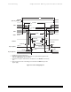
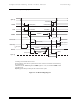
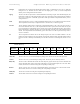
NOTE 1
NOTE 4
NOTE 1
NOTE 4
t
c
W
t
h
(CE)
t
en
(OE)
t
dis
(OE)
t
su
(OE-WE)
t
dis
(WE)
t
h
(D)
t
h
(OE-WE)
t
rec
(WE)
t
en
(WE)
DATA INPUT ESTABLISHED
t
su
(D-WEH)
NOTE 2
NOTE 3
t
w
(WT)
t
v
(WT)
t
v
(WT-WE)
t
w
(WE)
t
su
(A-WEH)
t
su
(A)
t
su
(CE-WEH)
t
su
(CE)
A[25::0], REG#
CE#
OE#
WE#
WAIT#
D[15::0](Din)
D[15::0](Dout)
1. Shaded areas may be high or low.
2. When the data I/O pin is in the output state, no signals shall be applied to the
data pins (D[15::0]) by the host system
3. Minimum write pulse width must be met whether or not WAIT# is asserted by
card.
4. May be high or low for write timing, but restrictions on OE# from previous
figures apply.
Figure 4-2 Write Timing Diagram