
Product manual

CompactFlash Memory Card Product Manual Preliminary
SanDisk CompactFlash Memory Card Product Manual Rev. 8 © 2001 SANDISK CORPORATION
46
5.2 Contiguous I/O Mapped Addressing
When the system decodes a contiguous block of
I/O registers to select the CompactFlash Memory
Card, the registers are accessed in the block of I/O
space decoded by the system as follows:
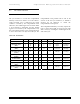
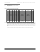
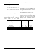
Table 5-3 Contiguous I/O Decoding
-REG A3 A2 A1 A0 Offset -IORD=0 -IOWR=0 Notes
0 0 0 0 0 0 Even RD Data Even WR Data 1
0 0 0 0 1 1 Error Features 2
0 0 0 1 0 2 Sector Count Sector Count
0 0 0 1 1 3 Sector No. Sector No.
0 0 1 0 0 4 Cylinder Low Cylinder Low
0 0 1 0 1 5 Cylinder High Cylinder High
0 0 1 1 0 6 Select Card /Head Select Card/Head
0 0 1 1 1 7 Status Command
0 1 0 0 0 8 Dup Even RD Data Dup. Even WR Data 2
0 1 0 0 1 9 Dup. Odd RD Data Dup. Odd WR Data 2
0 1 1 0 1 D Dup. Error Dup. Features 2
0 1 1 1 0 E Alt Status Device Ctl
0 1 1 1 1 F Drive Address Reserved
Notes: 1. Register 0 is accessed with -CE1 low and -CE2 low (and A0 = Don't Care) as a word register on the combined Odd
Data Bus and Even Data Bus (D15-D0). This register may also be accessed by a pair of byte accesses to the offset 0
with -CE1 low and -CE2 high. Note that the address space of this word register overlaps the address space of the Error
and Feature byte-wide registers that lie at offset 1. When accessed twice as byte register with -CE1 low, the first byte
to be accessed is the even byte of the word and the second byte accessed is the odd byte of the equivalent word access.
A byte access to register 0 with -CE1 high and -CE2 low accesses the error (read) or feature (write) register.
2. Registers at offset 8, 9 and D are non-overlapping duplicates of the registers at offset 0 and 1.
Register 8 is equivalent to register 0, while register 9 accesses the odd byte. Therefore, if the registers are byte
accessed in the order 9 then 8 the data will be transferred odd byte then even byte.
Repeated byte accesses to register 8 or 0 will access consecutive (even than odd) bytes from the data buffer. Repeated
word accesses to register 8, 9 or 0 will access consecutive words from the data buffer. Repeated byte accesses to
register 9 are not supported. However, repeated alternating byte accesses to registers 8 then 9 will access consecutive
(even then odd) bytes from the data buffer. Byte accesses to register 9 access only the odd byte of the data.
3. Address lines which are not indicated are ignored by the CompactFlash Memory Card for accessing all the registers
in this table.