
User Manual

Product Specifications
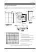
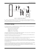
2-4 TriFlash with SD Interface Product Manual (Preliminary), Rev. 1.2 © 2002/2003 SANDISK CORPORATION
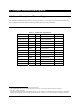
Dimension in mm Dimension in inch
Symbol MIN NOM MAX Min NOM MAX
A --- --- 1.10 --- --- 0.043
A1 0.32 0.35 0.38 0.013 0.014 0.015
A2 0.62 0.67 0.72 0.024 0.026 0.028
D 11.90 12.00 12.10 0.469 0.472 0.476
E 9.90 10.00 10.10 0.390 0.394 0.398
D1 --- 7.00 --- --- 0.276 ---
E1 --- 7.00 --- --- 0.276 ---
e --- 1.00 --- --- 0.039 ---
b 0.40 0.45 0.50 0.016 0.018 0.020
aaa 0.10 0.004
bbb 0.10 0.004
ddd 0.15 0.006
eee 0.25 0.010
fff 0.10 0.004
MD/ME 8/8 8/8
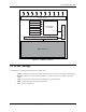
NOTE:
1. Controlling Dimension: Millimeter.
2. Primary Datum C and seating plane are defined by the
spherical crowns of the solder balls.
3. Dimensions b is measured at the maximum solder ball
diameter, parallel to Primary Datum C.
4. There shall be a minimum clearance of 0.25mm between
the edge of the solder ball and the body edge.
5. Reference document: JEDEC MO-205.
6. The pattern of Pin 1 Fiducial is for reference only.
DETAIL: B
DETAIL: A
A1
"A"
O fff M
C A B
C
Oeee M
12345678
H
G
F
E
D
C
B
A
"B"
D1
E1
B
A
1
2
(NOTE 6)
(NOTE 3)
b
Cavity
Seating Plane
Solder Ball
(NOTE 2)
A2
A1
A
C
bbb C
ddd C
A
B
aaa
D
E
aaa
e
Figure 2-2. TriFlash Physical Specifications—12 X 10mm Package