
User Manual

TriFlash Interface Description
TriFlash with SD Interface Product Manual (Preliminary), Rev. 1.2 © 2002/2003 SANDISK CORPORATION
3-3
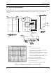
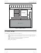
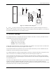
Memory Core
Card Interface
Controller
OCR[31:0]
CID[127:0]
RCA[15:0]
DSR[15:0]
CSD[127:0]
SCR[63:0]
reset
Memory Core Interface reset
Power Connection
DAT2 CD/DAT3 CMD RDY/BSY V
DD
CLK RSTB WPB DAT0 DAT1
Interface Driver
Figure 3-1. TriFlash Architecture
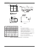
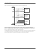
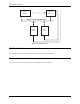
3.2. SD Bus Topology
The SD bus has six communication lines and three supply lines:
• CMD—Command is a bi-directional signal. (Host and device drivers are operating in push pull mode.)
• DAT0-3—Data lines are bi-directional signals. (Host and device drivers are operating in push pull
mode.)
• CLK—Clock is a host to devices signal. (CLK operates in push pull mode.)
• VDD—VDD is the power supply line for all devices.
• VSS—VSS are ground lines.