
User Manual

TriFlash Interface Description
3-16 TriFlash with SD Interface Product Manual (Preliminary), Rev. 1.2 © 2002/2003 SANDISK CORPORATION
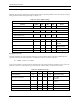
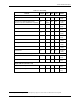
Name Field Width Cell Type CSD-Slice CSD Value CSD Code
File format group FILE_FORMAT_GRP 1 R/W(1) [15:15] 0 0b
copy flag (OTP) COPY 1 R/W(1) [14:14] Not Original 1b
permanent write protection PERM_WRITE_PROTECT 1 R/W(1) [13:13] Not Protected 0b
temporary write protection TMP_WRITE_PROTECT 1 R/W [12:12] Not Protected 0b
File format FILE_FORMAT 2 R/W(1) [11:10] HD w/partition 00b
Reserved 2 R/W [9:8] - 00b
CRC CRC 7 R/W [7:1] - CRC7
not used, always’1’ - 1 - [0:0] - 1b
The following sections describe the CSD fields and the relevant data types. If not explicitly defined otherwise, all
bit strings are interpreted as binary coded numbers starting with the left bit first.
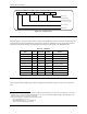
CSD_STRUCTURE—describes the version of the CSD structure.
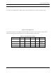
Table 3-11. CSD Register Structure
CSD_STRUCTURE CSD Structure Version Valid for SD Physical Specification Version
0 CSD version No. 1.0 Version 1.0-1.01
1-3 Reserved
TAAC—Defines the asynchronous part (relative to the TriFlash clock (CLK)) of the read access time.
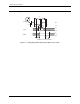
Table 3-12. TAAC Access Time Definition
TAAC Bit Position Code
2:0 time unit:
0=1ns, 1=10ns, 2=100ns, 3=1µms, 4=10µms, 5=100µms,
6=1ms, 7=10ms
6:3 time value:
0=Reserved, 1=1.0, 2=1.2, 3=1.3, 4=1.5, 5=2.0, 6=2.5, 7=3.0,
8=3.5, 9=4.0, A=4.5, B=5.0, C=5.5, D=6.0, E=7.0, F=8.0
7 Reserved
NSAC—Defines the worst case for the clock dependent factor of the data access time. The unit for NSAC is 100
clock cycles. Therefore, the maximal value for the clock dependent part of the read access time is 25.5k clock
cycles.
The total read access time N
AC
as expressed in Table 4-18 is the sum of TAAC and NSAC. It has to be computed by
the host for the actual clock rate. The read access time should be interpreted as a typical delay for the first data bit of
a data block from the end bit on the read commands.
TRAN_SPEED—Table 3-13 defines the maximum data transfer rate TRAN_SPEED.