
User Manual


Secure Digital (SD) Bus Protocol Description
TriFlash with SD Interface Product Manual (Preliminary), Rev. 1.2 © 2002/2003 SANDISK CORPORATION
4-31
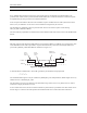
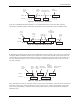
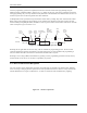
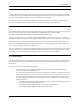
All previous examples dealt with the scenario of the host stopping the data transmission during an active data
transfer. The following two diagrams describe a scenario of receiving the stop transmission between data blocks. In
the first example the device is busy programming the last block while in the second the device is idle. However,
there are still unprogrammed data blocks in the input buffers. These blocks are being programmed as soon as the
stop transmission command is received and the device activates the busy signal.
<--Host Command--> <N
cr
Cycles>
<----Device response----> <Host Cmnd>
CMD S T content CRC E Z Z P * * * P S T content CRC E S T Content
<----------Device is programming---------->
DAT S L * * * * * * * * * * * * * * * * * * * * * * * ** ** * * * * * * * * * L E Z Z Z Z Z Z Z Z
Figure 4-24. Stop Transmission Received After Last Data Block. Device is Busy Programming
<--Host Command--> <N
cr
Cycles>
<----Device response----> <Host Cmnd>
CMD S T content CRC E Z Z P * * * P S T content CRC E S T Content
<----------Device is programming---------->
DAT Z Z Z Z Z Z Z Z Z Z Z S L * * * * * * * * * * * * * * * * * * * * * * * * L E Z Z Z Z Z Z Z Z
Figure 4-25. Stop Transmission Received After Last Data Block. Device becomes Busy
Erase, Set and Clear Write Protect Timing
The host must first tag the start (CMD32) and end (CMD33) addresses of the range to be erased. The erase
command (CMD38), once issued, will erase all the selected write blocks. Similarly, set and clear write protect
commands start a programming operation as well. The device will signal “busy” (by pulling the DAT line low) for
the duration of the erase or programming operation. The bus transaction timings are the same as given for stop tran
command.
Reselecting a Busy Device
When a busy device, which is currently in the dis state, is reselected it will reinstate its busy signaling on the data
line. The timing diagram for this command/response/busy transaction is the same as given for stop tran command.
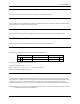
4.11.4. Timing Values
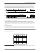
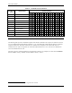
Table 4-18 defines all timing values.
Table 4-18. Timing Values
Min. Max. Unit
N
CR
2 64 Clock Cycles
N
ID
5 5 Clock Cycles
N
AC
2
See footnote
12
Clock Cycles
N
RC
8 - Clock Cycles
N
CC
8 - Clock Cycles
N
WR
2 - Clock Cycles
12
N
AC
maximum value shall be calculated using the following equation: MIN [([TAAC ∗ f + NSAC ∗ 100] ∗ 100), (100ms ∗ f)].