
User Manual

Introduction to the TriFlash with SD Interface
TriFlash with SD Interface Product Manual (Preliminary), Rev. 1.2 © 2002/2003 SANDISK CORPORATION
1-3
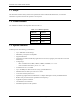
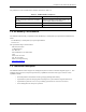
The performance of the communication channel is described in Table 1-2.
Table 1-2. SD Bus/SPI Bus Comparison
TriFlash Using SD Bus TriFlash Using SPI Bus
Six-wire communication channel (clock, command, 4
data lines).
Three-wire serial data bus (Clock, dataIn, dataOut) + card
specific CS signal (hardwired card selection).
Error-protected data transfer. Optional non-protected data transfer mode available.
Single or multiple block oriented data transfer. Single or multiple block oriented data transfer.
1.4. SD Memory Card Standard
The SanDisk TriFlash is fully compatible with the SD Memory Card Physical Layer Specification standard listed
below:
The SD Memory Card Physical Layer System Specification
Version 1.01
This specification may be obtained from:
SD Card Association
53 Muckelemi St.
P.O. Box 189
San Juan Bautista, CA 95045-0189
USA
Phone: 831-623-2107
Fax: 831-623-2248
Email: rcreech@sdcard.org
http://www.sdcard.org
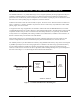
1.5. Functional Description
The SanDisk TriFlash contains a high level, intelligent subsystem as shown in the block diagram, Figure 1-1. This
intelligent (microprocessor) subsystem provides many capabilities not found in other types of devices. These
capabilities include:
• Host independence from details of erasing and programming flash memory.
• Sophisticated system for managing defects (analogous to systems found in magnetic disk drives).
• Sophisticated system for error recovery including a powerful error correction code (ECC).
• Power management for low power operation.