SanDisk CompactFlash Memory Card OEM Product Manual Version 12.0 Document No. 20-10-00038 02/2007 SanDisk Corporation Corporate Headquarters 601 McCarthy Boulevard Milpitas, CA 95035 (408) 801-1000 Phone (408) 801-8657 Fax www.sandisk.
SanDisk CompactFlash Card OEM Product Manual SanDisk® Corporation general policy does not recommend the use of its products in life support applications where in a failure or malfunction of the product may directly threaten life or injury. Per SanDisk Terms and Conditions of Sale, the user of SanDisk products in life support applications assumes all risk of such use and indemnifies SanDisk against all damages. Security safeguards, by their nature, are capable of circumvention.
SanDisk CompactFlash Card OEM Product Manual –This page intentionally left blank– 02/07, Rev. 12.
Table of Contents CHAPTER 1 Introduction . . . . . . . . . . . . . . . . . . . . . . . . . . . . . . . . . . . . . . . 1-1 General Description . . . . . . . . . . . . . . . . . . . . . . . . . . . . . . . . . . . . . 1-1 Features . . . . . . . . . . . . . . . . . . . . . . . . . . . . . . . . . . . . . . . . . . . . . . 1-2 Scope . . . . . . . . . . . . . . . . . . . . . . . . . . . . . . . . . . . . . . . . . . . . . . . . 1-2 CompactFlash Standard . . . . . . . . . . . . . . . . . . . . . . . . . . . .
Table of Contents SanDisk CompactFlash Card OEM Product Manual Memory Mapped Addressing . . . . . . . . . . . . . . . . . . . . . . . . . . . . . .4-3 True IDE Mode Addressing . . . . . . . . . . . . . . . . . . . . . . . . . . . . . . . .4-4 ATA Registers . . . . . . . . . . . . . . . . . . . . . . . . . . . . . . . . . . . . . . . . . .4-4 CHAPTER 5 ATA Command Description . . . . . . . . . . . . . . . . . . . . . . . . . . 5-1 ATA Command Set . . . . . . . . . . . . . . . . . . . . . . . . . . . . . .
Introduction CHAPTER 1 1.1 General Description SanDisk CompactFlash® Memory Card products provide high capacity solid-state flash memory that electrically complies with the Personal Computer Memory Card International Association ATA (PC Card ATA) standard. (In Japan, the applicable standards group is JEIDA.) The CompactFlash Memory Card Series also supports a True IDE Mode that is electrically compatible with an IDE disk drive.
Introduction 1.2 SanDisk CompactFlash Card OEM Product Manual Features SanDisk CompactFlash Memory cards provide the following system features: • • • • • • • • • • • • • • • 1.3 Up to 16 GB of mass storage data PC Card ATA protocol compatible True IDE Mode compatible Very low CMOS power Very high performance Very rugged Low weight Noiseless Low Profile +5 Volts or +3.
SanDisk CompactFlash Card OEM Product Manual 1.5 Introduction PCMCIA Standard SanDisk CompactFlash Memory cards are fully electrically compatible with the PCMCIA specifications listed below: • PCMCIA PC Card Standard, 7.0, February 1999 • PCMCIA PC Card ATA Specification, 7.0, February 1999 These specifications may be obtained from: PCMCIA 2635 N. First Street, Suite 209 San Jose, CA 95131 USA Phone: 408-433-2273 Fax: 408-433-9558 1.
Introduction 1.7.1 SanDisk CompactFlash Card OEM Product Manual Technology Independence The 512-byte sector size of the CompactFlash Memory Card is the same as that in an IDE magnetic disk drive. To write or read a sector (or multiple sectors), the host computer software simply issues a Read or Write command to the card. This command contains the address and the number of sectors to write/read. The host software then waits for the command to complete.
SanDisk CompactFlash Card OEM Product Manual 1.7.5 Introduction Automatic Sleep Mode A unique feature of the SanDisk CompactFlash Memory Card is automatic entrance and exit from sleep mode. Upon completion of a command, the card will enter sleep mode to conserve power if no further commands are received within 5 msec. The host does not have to take any action for this to occur. In most systems, the CompactFlash Memory Card is in sleep mode except when the host is accessing it, thus conserving power.
Introduction SanDisk CompactFlash Card OEM Product Manual –This page intentionally left blank– 02/07, Rev. 12.
Product Specifications CHAPTER 2 For all the following specifications, values are defined at ambient temperature and nominal supply voltage unless otherwise stated. 2.1 System Environmental Specifications Table 2-1 contains environmental specifications which include temperature, humidity, acoustic noise, vibration, shock and altitude. Table 2-1 Environmental Specifications Temperature Humidity Acoustic Noise Vibration Shock Altitude (relative to sea level) 2.
Product Specifications SanDisk CompactFlash Card OEM Product Manual Sleep mode currently is specified under the condition that all card inputs are static CMOS levels and in a "Not Busy" operating state. Table 2-2 Power Requirements DC Input Voltage (Vcc) 100 mV max. ripple (p-p) a Memory Subsystem 3.3V +/- 5% 5V +/- 10% Up to 512 MB 300 µ 500 µ 1.0 GB 600 µ 800 µ 1 mA 1.2 mA 50 mA 55 mA CompactFlash Memory Card Sleep Over 1.
SanDisk CompactFlash Card OEM Product Manual 2.3 Product Specifications System Performance All performance timings assume the CompactFlash Memory Card Series controller is in the default (i.e., fastest) mode. Table 2-3 Performance CompactFlash Memory Card Start-up Times Sleep to Write 2.5 ms maximum Sleep to Read 20 ms maximum Reset to Ready Active to Sleep Delay Data Transfer Rate To/From Flash Data Transfer Rate To/From Host 50 ms typical; 400 ms maximum Programmable 20.0 MB/sec burst 16.
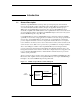
Product Specifications 2.4 SanDisk CompactFlash Card OEM Product Manual System Reliability Table 2-4 Reliability >1,000,000 hours MTBF (@ 25 C) None Preventative Maintenance <1 non-recoverable error in 1014 bits read Data Reliability <1 erroneous correction in 1020 bits read 2.5 Physical Specifications Refer to Table 2-5 and see Figure 2-1 for CompactFlash Memory Card physical specifications and dimensions. Table 2-5 Weight Length Width Thickness 02/07, Rev. 12.
SanDisk CompactFlash Card OEM Product Manual Figure 2-1 © 2007 SanDisk Corporation Product Specifications CompactFlash Memory Card Dimensions 2-5 Rev. 12.
Product Specifications SanDisk CompactFlash Card OEM Product Manual –This page intentionally left blank– 02/07, Rev. 12.
Interface Description CHAPTER 3 3.1 Physical Description The host connects to SanDisk CompactFlash Memory cards using a standard 50-pin connector consisting of two rows of 25 female contacts each on 50 mil (1.27 mm) centers. 3.1.1 Pin Assignments and Types The signal/pin assignments are listed in Table 3-1. Low active signals have a "-" prefix. Pin types are Input, Output or Input/Output. Sections 3.3.1 and 3.3.2 define the DC characteristics for all input and output type structures..
Interface Description SanDisk CompactFlash Card OEM Product Manual PC Card I/O Pin Assignments are contained in Table 3-2. Table 3-2 PC Card I/O Mode Pin Assignments Pin No. Signal Name Pin No.
SanDisk CompactFlash Card OEM Product Manual Table 3-3 3.2 Interface Description True IDE Mode Pin Assignments Pin No. Signal Name Pin Type 9 -ATA SEL I Pin No.
Interface Description SanDisk CompactFlash Card OEM Product Manual The SanDisk CompactFlash Memory Card signals are described in Table 3-4. Table 3-4 Signal Description Signal Name Dir.
SanDisk CompactFlash Card OEM Product Manual Table 3-4 Interface Description Signal Description Signal Name Dir. Pin Description -CSEL (True IDE Mode) D15-D00 (PC Card Memory Mode) (PC Card I/O Mode) This internally pulled up signal is used to configure this device as a master or slave when configured in the True IDE Mode. When this pin is grounded, this device is configured as a master. When the pin is open, this device is configured as a slave.
Interface Description SanDisk CompactFlash Card OEM Product Manual Table 3-4 Signal Description Signal Name Dir. Pin -IOWR (PC Card I/O Mode) (True IDE Mode) -OE (PC Card Memory Mode) The I/O write strobe pulse is used to clock I/O data on the Card Data bus into the card controller registers when the card is configured to use the I/O interface. The clocking will occur on the negative to positive edge of the signal (trailing edge).
SanDisk CompactFlash Card OEM Product Manual Table 3-4 Interface Description Signal Description Signal Name Dir. Pin Description This signal is used by the host in response to DMARQ to initiate DMA transfers. NOTE: This signal may be negated by the host to suspend the DMS transfer in process. For Multiword DMA transfers, the device may negate DMARQ with the tL specified time once the DMACK- is asserted and reasserted again at a later time to resume DMA operation.
Interface Description SanDisk CompactFlash Card OEM Product Manual Table 3-4 Signal Description Signal Name 3.3 Dir. Pin Description -IOIS16 (PC Card I/O Mode) I/O Operation–When the card is configured for I/O Operation, pin 24 is used for the -I/O Selected is 16 Bit Port (-IOIS16) function. A low signal indicates that a 16-bit or odd-byte only operation can be performed at the addressed port.
SanDisk CompactFlash Card OEM Product Manual Interface Description Table 3-6 defines the input characteristics of the parameters in Table 3-5. Table 3-6 Input Characteristics Min. 3.3.2 Typ. Max. Min. VCC = 3.3V Typ. Type Parameter Symbol 1 Input Voltage Vih CMOS Vil 2 Input Voltage Vih CMOS Vil 3 Input Voltage Vth 1.8 2.8 CMOS Schmitt Trigger Vtl 1.0 2.0 Max. VCC = 5.0V 2.4 Unit 4.0 V 0.6 1.5 0.8 2.0 V 0.6 0.
Interface Description 3.3.3 SanDisk CompactFlash Card OEM Product Manual Power Up/Power Down Timing The timing specification in Table 3-9 was defined to permit peripheral cards to perform powerup initialization. Table 3-9 Power Up/Power Down Timing Item Value a CE Signal Level Symbol Condition Min. Max. Unit Vi (CE) 0V
SanDisk CompactFlash Card OEM Product Manual Figure 3-2 Interface Description Power Up/Power Down Timing for Systems not supporting RESET tpr VCC VCC Min. tSU(VCC) VIH 2V -CE1, -CE2 Always Hi-z from system Supplied by pull-up resistor on card (if present) RESET tpf VCC VCC Min. trec VIH 2V -CE1, -CE2 3.3.4 Common Memory Read Timing Table 3-10 contains common memory read timing specifications for all types of memory. NOTE: All timings measured at the CompactFlash Memory Card.
Interface Description SanDisk CompactFlash Card OEM Product Manual Table 3-10 Common Memory Read Timing Specification 100 ns Speed Version Item Address Hold Time Symbol IEEE Symbol Min. Max. th (A) tGHAX 15 --- Card Enable Setup Time tsu(CE) tELGL 0 --- Card Enable Hold Time th (CE) tGHEH 15 --- a. The -REG signal timing is identical to address signal timing 3.3.5 Common and Attribute Memory Write Timing The write timing specifications for Common and Attribute memory are the same.
SanDisk CompactFlash Card OEM Product Manual 3.3.6 Interface Description Attribute Memory Read Timing Specification Table 3-12 contains common memory write timing specifications for all types of memory. NOTE: SanDisk CompactFlash Memory cards do not assert the -WAIT signal. Table 3-12 Attribute Memory Read Timing Specification 300 ns Symbol IEEE Symbol Min. Max.
Interface Description SanDisk CompactFlash Card OEM Product Manual Figure 3-4 02/07, Rev. 12.0 Common and Attribute Memory Write Timing Diagram NOTE 1: Shaded areas may be high or low. NOTE 2: When the data I/O pins are in the output state, no signals shall be applied to the data pins (D[15::0]) by the host system NOTE 3: May be high or low for write timing, but restrictions on -OE from previous figures apply. NOTE 4: SanDisk CompactFlash Memory Cards do not assert the -WAIT signal.
SanDisk CompactFlash Card OEM Product Manual 3.3.8 Interface Description I/O Read (Input) Timing Specification Figure 3-5 I/O Read Timing Diagram NOTE 1: All timings are measured at the CompactFlash Memory Card. NOTE 2: Skews and delays from the host system driver/receiver to the card must be accounted for by the system design. NOTE 3: D[15::0] signifies data provided by the card to the host system. Table 3-13 contains the read input timing specifications.
Interface Description SanDisk CompactFlash Card OEM Product Manual Table 3-13 I/O Read (Input) Timing Specification Symbol Item IEEE Symbol Min. (ns) Max. (ns) -IOIS16 Delay falling from Address tdfIOIS16(ADR) tAVISL --- 35a -IOIS16 Delay rising from Address tdrIOIS16(ADR) tAVISH --- 35a a. The maximum load on -INPACK and -IOIS16 is 1 LSTTL with 50 pF total load. 3.3.9 I/O Write (Output) Timing Specification Figure 3-6 02/07, Rev. 12.
SanDisk CompactFlash Card OEM Product Manual Interface Description Table 3-14 contains the specification information related to the I/O Write Timing Diagram. Table 3-14 I/O Write Timing Specification Item Symbol IEEE Symbol Min. (ns) Max.
Interface Description SanDisk CompactFlash Card OEM Product Manual Figure 3-7 Register Transfer to/from Device NOTE 1: Device address consists of signals -CS0, -CS1 and -DA(2:0). NOTE 2: Data consists of DD(7:0). Table 3-15 Register Transfer to/from Device Mode 4 (ns) PIO Timing Parameters t0a Cycle time (min.) 120 t1 Address valid to IORD-/IOWR- setup (min.) 25 t2a IORD-/IOWR- pulse width 8-bit (min.) 70 t2ia IORD-/IOWR- recovery time (min.) 25 t3 IOWR- data setup (min.
SanDisk CompactFlash Card OEM Product Manual Interface Description • PIO Data Transfers Figure 3-8 defines the relationships between the interface signals for PIO data transfers. For PIO Modes 3 and above, the minimum value of t0 is specified by Word 68 in the IDENTIFY DEVICE parameter list. Table 3-16 defines the minimum value that will be placed in Word 68. Figure 3-8 PIO Data Transfer to/from Device NOTE 1: Device address consists of signals -CS0, -CS1 and -DA(2:0).
Interface Description SanDisk CompactFlash Card OEM Product Manual The PIO data transfer parameters are defined in Table 3-16. NOTE: SanDisk CompactFlash Memory cards do not assert an -IORDY signal. Table 3-16 PIO Data Transfer to/from Device PIO Timing Parameters Mode 0 (ns) Mode 1 (ns) Mode 2 (ns) Mode 3 (ns) Mode 4 (ns) t0a Cycle time (min.) 600 383 240 180 120 t1 Address valid to IORD-/IOWR- setup (min.) 70 50 30 30 25 t2a IORD-/IOWR- pulse width 16-bit (min.
SanDisk CompactFlash Card OEM Product Manual Interface Description In addition, these registers provide a method for accessing status information about the card that may be used to arbitrate between multiple interrupt sources on the same interrupt level or to replace status information that appears on dedicated pins in memory cards that have alternate use in I/O cards.
Interface Description SanDisk CompactFlash Card OEM Product Manual Decoding for the configuration registers is defined in Table 3-18. Table 3-18 3.4.
SanDisk CompactFlash Card OEM Product Manual 3.4.2 Interface Description Configuration Option Register (Address 200h in Attribute Memory) The Configuration Option Register is used to configure the card’s interface, address decoding and interrupt and to issue a soft reset to the CompactFlash Memory Card.
Interface Description SanDisk CompactFlash Card OEM Product Manual Card Configuration and Status Register (con’t) 3.4.4 Bit Name Description D7 Changed Indicates that one or both of the Pin Replacement Register CRdy, or CWProt bits are set to "1". When the Changed bit is set, -STSCHG Pin 46 is held low if the SigChg bit is a "1" and the card is configured for the I/O interface.
SanDisk CompactFlash Card OEM Product Manual Interface Description Pin replacement changed bit/mask values are contained in Table 3-21. Table 3-21 Pin Replacement Changed Bit/Mask Bit Values Written by Host 3.4.5 Initial Value of (C) Status “C” Bit “M” Bit Final “C” Bit 0 X 0 0 Comments Unchanged 1 X 0 1 Unchanged X 0 1 0 Cleared by host X 1 1 1 Set by host Socket and Copy Register (Address 206h in Attribute Memory) This register contains additional configuration information.
Interface Description SanDisk CompactFlash Card OEM Product Manual Table 3-22 Common Memory Function Function Code 3.
ATA Register Set and Protocol CHAPTER 4 SanDisk CompactFlash Memory cards can be configured as a high performance I/O device through the following ways: • Standard PC-AT disk I/O address spaces 1F0h-1F7h, 3F6h-3F7h (primary); 170h-177h, 376h-377h (secondary) with IRQ 14 (or other available IRQ). • Any system decoded 16-byte I/O block using any available IRQ. • Memory space.
ATA Register Set and Protocol SanDisk CompactFlash Card OEM Product Manual a. Register 0 is accessed with -CE1 low and -CE2 low (and A0 = Do not care) as a word register on the combined Odd Data Bus and Even Data Bus (D15-D0). This register may also be accessed by a pair of byte accesses to the offset 0 with -CE1 low and -CE2 high. Note that the address space of this word register overlaps the address space of the Error and Feature byte-wide registers that lie at off set 1.
SanDisk CompactFlash Card OEM Product Manual 4.3 ATA Register Set and Protocol Memory Mapped Addressing When CompactFlash Memory Card registers are accessed via memory references, they appear in the common memory space window: 0-2K bytes as shown in Table 4-4.
ATA Register Set and Protocol 4.4 SanDisk CompactFlash Card OEM Product Manual True IDE Mode Addressing When a CompactFlash Memory Card is configured in the True IDE Mode the I/O decoding is as listed in Table 4-5. Table 4-5 4.5 True IDE Mode I/O Decoding -CE2 -CE1 A2 A1 A0 1 0 0 0 0 Even RD Data -IORD=0 -IOWR=0 1 0 0 0 1 Error Register Features 1 0 0 1 0 Sector Count Sector Count 1 0 0 1 1 Sector No. Sector No.
SanDisk CompactFlash Card OEM Product Manual Table 4-6 Data Register Data Register 4.5.2 ATA Register Set and Protocol CE2 CE1 A0 Offset Data Bus Error/Feature Register 0 1 X 1 D15-D0 Error/Feature Register 0 0 X Dh D15-D0 Error Register (Address–1F1[171]; Offset 1, 0Dh Read Only) This register contains additional information about the source of an error when an error is indicated in bit 0 of the Status Register.
ATA Register Set and Protocol 4.5.6 SanDisk CompactFlash Card OEM Product Manual Cylinder Low (LBA 15-8) Register (Address–1F4[174]; Offset 4) This register contains the low order 8 bits of the starting cylinder address or bits 15-8 of the Logical Block Address. 4.5.7 Cylinder High (LBA 23-16) Register (Address–1F5[175]; Offset 5) This register contains the high order bits of the starting cylinder address or bits 23-16 of the Logical Block Address. 4.5.
SanDisk CompactFlash Card OEM Product Manual 4.5.9 ATA Register Set and Protocol Status & Alternate Status Registers (Address–1F7[177]&3F6[376]; Offsets 7 & Eh) These registers return the card status when read by the host. Reading the Status Register clears a pending interrupt while reading the Auxiliary Status Register does not. The meaning of the status bits are described as follows: 4.5.
ATA Register Set and Protocol SanDisk CompactFlash Card OEM Product Manual Device Control Register (con’t) 4.5.11 Bit Name Description D7 X Don’t care. D6 X Don’t care. D5 X Don’t care. D4 X Don’t care. D3 1 Bit ignored by the card. D2 SW Rst Set to 1 in order to force the card to perform an AT Disk controller Soft Reset operation. This does not change the PCMCIA Card Configuration registers as a hardware reset does. The card remains in Reset until this bit is reset to “0”.
SanDisk CompactFlash Card OEM Product Manual ATA Register Set and Protocol Card (Drive) Address Register (con’t) Bit Name Description D7 X This bit is unknown. Implementation Note: Conflicts may occur on the host data bus when this bit is provided by a Floppy Disk Controller operating at the same addresses as the CompactFlash Memory Card. Following are some possible solutions to this problem for the PCMCIA implementation: 1. Locate the CompactFlash Memory Card at a non-conflicting address, i.e.
ATA Register Set and Protocol SanDisk CompactFlash Card OEM Product Manual –This page intentionally left blank– 02/07, Rev. 12.
ATA Command Description CHAPTER 5 This section defines the software requirements and the format of commands the host sends to CompactFlash Memory cards. Commands are issued to the card by loading the required registers in the command block with the supplied parameters, and then writing the command code to the Command Register. The manner in which a command is accepted varies.
ATA Command Description SanDisk CompactFlash Card OEM Product Manual Table 5-1 Primary and Secondary I/O Decoding Class Command Code FR SC SN CY DH LBA 1 Set Multiple Mode C6h - Y - - D - 1 Set Sleep Mode E6h or 99h - - - - D - 1 Stand By E2h or 96h - - - - D - 1 Stand By Immediate E0h or 94h - - - - D - 87h - Y Y Y Y Y 1 b Wear Level F5h - - - - Y - 2 Write Buffer E8h - - - - D - 2 Write DMA CA or CB - Y Y Y Y Y 2 Write L
SanDisk CompactFlash Card OEM Product Manual ATA Command Description If the card is in Idle mode, it sets BSY, sets the Sector Count Register to FFh, clears BSY and generates an interrupt. Table 5-2 Check Power Mode Bit 7 6 5 Command (7) 3 2 1 0 E5H or 98H C/D/H (6) 5.1.2 4 X Drive X Cyl High (5) X Cyl Low (4) X Sec Num (3) X Sec Cnt (2) X Feature (1) X Execute Drive Diagnostic–90H This command performs the internal diagnostic tests implemented by the CompactFlash cards.
ATA Command Description 5.1.3 SanDisk CompactFlash Card OEM Product Manual Erase Sector(s)–C0H This command is no longer recommended. There is essentially no net gain in the use of the Erase Sectors Command and/or the Write Without Erase Commands. This command is supported to guarantee backward compatibility. Table 5-5 Erase Sectors Bit 7 6 5 4 1 LBA 1 Drive Command (7) C/D/H (6) 5.1.
SanDisk CompactFlash Card OEM Product Manual 5.1.5 ATA Command Description Identify Device–ECH The Identify Drive command enables the host to receive parameter information from a CompactFlash Memory Card. This command has the same protocol as the Read Sector(s) command. The parameter words in the buffer have the arrangement and meanings defined in Table 5-8. All reserved bits or words are “0”.
ATA Command Description Table 5-8 Word Address 02/07, Rev. 12.
SanDisk CompactFlash Card OEM Product Manual Table 5-8 ATA Command Description Identify Device Information Word Address Default Value Total Bytes 163 00XXh 2 CF Advanced True IDE Timing Mode Capability and Setting 164 001Bh 2 CF Advanced PCMCIA I/O and Memory Timing Mode Capability 165-175 0000h 22 Reserved for assignment by the CFA 176-255 0000h 140 Reserved Data Field Type Information a. Multiword DMA is supported by SanDisk PCMCIA.
ATA Command Description SanDisk CompactFlash Card OEM Product Manual Word 21: Buffer Size. This field defines the buffer capacity of 2 sectors or 1 kilobyte of SRAM. Word 22: ECC Count. This field defines the number of ECC bytes used on each sector in the Read and Write Long commands. Words 23-26: Firmware Revision. This field contains the revision of the firmware for this product. Words 27-46: Model Number.
SanDisk CompactFlash Card OEM Product Manual ATA Command Description Word 53: Translation Parameters Valid. Bit 0 of this field is set, indicating that words 54 to 58 are valid and reflect the current number of cylinders, heads and sectors. Bit 1 is also set, indicating values in words 64 through 70 are valid. Words 54-56: Current Number of Cylinders, Heads, Sectors/Track. These fields contain the current number of user addressable cylinders, heads, and sectors/track in the current translation mode.
ATA Command Description SanDisk CompactFlash Card OEM Product Manual Word 68: Minimum PIO Transfer Cycle Time With Flow Control. This field indicates in nanoseconds, the minimum cycle time the card supports while performing data transfers using flow control. Words 82-84: Features/Command Sets Supported. Words 82, 83, and 84 indicate the features and command sets supported.
SanDisk CompactFlash Card OEM Product Manual ATA Command Description Bits 0-13 of word 87 are reserved. Bit 14 of word 87 will be set to one and bit 15 of word 87 will be cleared to zero to provide indication that the features/command sets enabled words are valid. The values in these words should not be depended upon by host implementers.
ATA Command Description SanDisk CompactFlash Card OEM Product Manual • Bits 2-0: Advanced True IDE PIO Mode Support Indicates the maximum True IDE PIO mode supported by the card. Value Maximum PIO Mode Timing Supported 0 Specified in Word 64 1 PIO Mode 5 2 3-7 PIO Mode 6 Reserved • Bits 5-3: Advanced True IDE Multiword DMA Mode Support Indicates the maximum True IDE Multiword DMA mode supported by the card.
SanDisk CompactFlash Card OEM Product Manual ATA Command Description Word 164: CF Advanced PCMCIA I/O and Memory Timing Mode Capabilities and Set tings. This word describes the capabilities and current settings for CFA defined advanced timing modes using the Memory and PCMCIA I/O interface. • Bits 2-0: Maximum Advanced PCMCIA I/O Mode Support Indicates the maximum I/O timing mode supported by the card.
ATA Command Description 5.1.7 SanDisk CompactFlash Card OEM Product Manual Idle Immediate–95H, E1H This command causes the card to set BSY, enter the Idle (Read) mode, clear BSY and generate an interrupt. Table 5-14 Idle Immediate Bit 7 6 5 Command (7) 3 2 1 0 E1H or 95H C/D/H (6) 5.1.
SanDisk CompactFlash Card OEM Product Manual 5.1.9 ATA Command Description Read Buffer–E4H The Read Buffer command enables the host to read the current contents of the card's sector buffer. This command has the same protocol as the Read Sector(s) command. Table 5-16 Read Buffer Bit 7 6 5 4 Command (7) C/D/H (6) 5.1.
ATA Command Description 5.1.11 SanDisk CompactFlash Card OEM Product Manual Read Multiple–C4H The Read Multiple command performs similarly to the Read Sectors command. Interrupts are not generated on every sector, but on the transfer of a block, which contains the number of sectors defined by a Set Multiple, command.
SanDisk CompactFlash Card OEM Product Manual 5.1.12 ATA Command Description Read Long Sector–22H, 23H The Read Long command performs similarly to the Read Sector(s) command except that it returns 516 bytes of data instead of 512 bytes. During a Read Long command, the card does not check the ECC bytes to determine if there has been a data error. Only single sector read long operations are supported.
ATA Command Description SanDisk CompactFlash Card OEM Product Manual When the requested sectors have been verified, the card clears BSY and generates an interrupt. Upon command completion, the Command Block registers contain the cylinder, head, and sector number of the last sector verified. If an error occurs, the verify terminates at the sector where the error occurs. The Command Block registers contain the cylinder, head and sector number of the sector where the error occurred.
SanDisk CompactFlash Card OEM Product Manual ATA Command Description Table 5-24 defines the valid extended error codes for the CompactFlash Memory Card Series product. The extended error code is returned to the host in the Error Register. This command must be the next command issued to the card following the command that returned an error.
ATA Command Description 5.1.18 SanDisk CompactFlash Card OEM Product Manual Set Features–EFH This command is used by the host to establish or select certain features. Table 5-26 Set Features Bit 7 6 5 Command (7) 4 3 2 1 0 EFH C/D/H (6) X Drive X Cyl High (5) X Cyl Low (4) X Sec Num (3) X Sec Cnt (2) Config Feature (1) Feature Table 5-27 defines all features that are supported. The 9AH feature is unique to CompactFlash Memory cards and are not part of the ATA Specification.
SanDisk CompactFlash Card OEM Product Manual ATA Command Description A host can choose the transfer mechanism by Set Transfer Mode and specifying a value in the Sector Count register. The upper 5 bits define the type of transfer and the low order 3 bits encode the mode value.
ATA Command Description SanDisk CompactFlash Card OEM Product Manual If the Sector Count Register contains a valid value and the block count is supported, the value is loaded for all subsequent Read Multiple and Write Multiple commands and execution of those commands is enabled. If a block count is not supported, an Aborted Command error is posted, and Read Multiple and Write Multiple commands are disabled.
SanDisk CompactFlash Card OEM Product Manual 5.1.21 ATA Command Description Standby–96H, E2H This command causes the card to set BSY, enter the Sleep mode (which corresponds to the ATA "Standby" Mode), clear BSY and return the interrupt immediately. Recovery from sleep mode is accomplished by simply issuing another command (reset is not required). Table 5-30 Standby Bit 7 6 5 Command (7) 3 2 1 0 E2H or 96H C/D/H (6) 5.1.
ATA Command Description SanDisk CompactFlash Card OEM Product Manual Table 5-33 represents the information in the buffer. This command is unique to SanDisk CompactFlash Memory cards. Table 5-33 Translate Sector Information Address 00 Head 01-02 Cylinder 03 Sector 04-07 LBA 08 Chip 09-0A Block 0B Page 0C-1FF 5.1.24 Information Reserved Wear Level–F5H This command is effectively a NOP command and only implemented for backward compatibility with earlier SanDisk SDP series products.
SanDisk CompactFlash Card OEM Product Manual 5.1.26 ATA Command Description Write DMA Command–CAH, CBH The Write DMA command in Table 5 33 executes in a similar manner to WRITE SECTOR(S) except for the following: • The host initialised the DMA channel prior to issuing the command. • Data transfers are qualified by DMARQ and are performed by the DMA channel. • The device issues only one interrupt per command to indicate that data transfer has termi nated and status is available.
ATA Command Description SanDisk CompactFlash Card OEM Product Manual DRQ qualification of the transfer is required only at the start of the data block, not on each sector. The block count of sectors to be transferred without intervening interrupts is programmed by the Set Multiple Mode command, which must be executed prior to the Write Multiple command.
SanDisk CompactFlash Card OEM Product Manual 5.1.29 ATA Command Description Write Multiple without Erase–CDH SanDisk does not recommend the use of this command in new designs but it is supported as a normal Write Sectors command for backward compatibility reasons. Table 5-39 Write Multiple w/out Erase Bit 7 6 5 4 Command (7) C/D/H (6) X LBA X Cyl High (5) 5.1.
ATA Command Description 5.1.31 SanDisk CompactFlash Card OEM Product Manual Write Sector(s) without Erase–38H SanDisk does not recommend the use of this command in new designs but it is supported as a normal Write Sectors command for backward compatibility reasons. Table 5-41 Write Sector(s) w/out Erase Bit 7 6 5 4 1 LBA 1 Drive Command (7) C/D/H (6) 5.1.
SanDisk CompactFlash Card OEM Product Manual 5.2 ATA Command Description Error Posting Table 5-43 summarizes the valid status and error value for all the ATA command set.
ATA Command Description SanDisk CompactFlash Card OEM Product Manual –This page intentionally left blank– 02/07, Rev. 12.
CIS Description CHAPTER 6 This section describes the Card Information Structure (CIS) for SanDisk CompactFlash Memory cards.
CIS Description SanDisk CompactFlash Card OEM Product Manual Table 6-1 Card Information Structure Attribute Offset Data 026h 00h 7 6 5 4 3 2 1 High Byte of PCMCIA Manufacturer’s Code 0 Content Description CIS Function Code of 0 because other High Byte of byte is JEDEC 1 byte PCMCIA Manufacturer’s ID Mfg ID 028h 01h Low Byte of Product Code SanDisk Code for Low Byte SDP Series Product Code 02Ah 04h High Byte of Product Code SanDisk Code for High Byte PC Card ATA Product
SanDisk CompactFlash Card OEM Product Manual Table 6-1 CIS Description Card Information Structure Attribute Offset Data 7 6 5 4 062h 14h W 12 NI PP 3 2 1 0 P RIA RIR SP 0 0 1 CIS Function No Wear Level & NO SanDisk D Vpp Fields, 1 to 4 N W: No Wear Level Bytes limited A 1 Content Description by link length 12: Vpp not used on 0 1 0 0 Write NI: -INPACK connected PP: Programmable Power PDNA: Pwr Down Not Abort--Cmd RIA: RBsy, ATBsy con nected RIR: RBsy Inhibited at
CIS Description SanDisk CompactFlash Card OEM Product Manual Table 6-1 Card Information Structure Attribute Offset Data 074h 01h 076h 7 6 5 4 3 2 1 0 Disk Function Extension Tuple Type Content Description CIS Function Extension Tuple Extension describes the Interface Tuple Type Protocol for Disk 01h Interface Type Code PC Card–ATA Interface Extension Info CISTPL_FUNCE Function Extension tuple Tuple Code Tuple has 3 Info Bytes Link Length 078h 22h 07Ah 03h 07Ch 02h Di
SanDisk CompactFlash Card OEM Product Manual Table 6-1 CIS Description Card Information Structure Attribute Offset Data 086h 01h 7 6 5 4 3 2 1 RFS RMS RAS 00 00 01 0 Content Description Size of Reserved Field CIS Function Size of is 0 Bytes Fields Byte Size of Register Mask (TPCC_SZ) is 1 Byte Size of Config Base Address is 2 Bytes RFS: Bytes in Reserved Field RMS: Bytes in Reg Mask–1 RAS: Bytes in Base Addr–1 088h 07h TPCC_LAST Entry with Config Index Last Entry of 07h is f
CIS Description SanDisk CompactFlash Card OEM Product Manual Table 6-1 Card Information Structure Attribute Offset Data 7 6 5 4 096h C0h W R P B 1 1 0 3 2 1 0 Interface Type Content Description Memory Only CIS Function TPCE_IF Interface(0), Bvd's and 0 wProt not used, Ready/-Busy and Wait for memory cycles active.
SanDisk CompactFlash Card OEM Product Manual Table 6-1 CIS Description Card Information Structure Attribute Offset Data 7 6 5 4 3 0A8h 21h X R P RO A 0 0 1 0 0 2 Content Description CIS Function T Power-Down and TPCE_MI 1 Twin Card.
CIS Description SanDisk CompactFlash Card OEM Product Manual Table 6-1 Card Information Structure Attribute Offset Data 7 6 0BEh C1h I D 1 5 4 3 2 1 0 Configuration Index 1 Content Description CIS Function I/O Mapped Contiguous TPCE_INDX 16 Registers 1 Configuration. Configuration Index for this entry is 1. Interface Byte follows this byte. Default Configuration, therefore is not dependent on previous Default Configuration.
SanDisk CompactFlash Card OEM Product Manual Table 6-1 CIS Description Card Information Structure Attribute Offset Data 7 0C8h 4Dh X Mantissa Exponent 0 9h = 4.5 5h = 1V X Mantissa Exponent 0 Bh = 5.5 5h = 1V X Mantissa Exponent Max. Average Current 0 Eh = 8.0 5h = 10 over 10 ms is 80 mA Current TPCE_IO 0CAh 0CCh 0CEh 5Dh 75h 64h 6 5 4 3 2 1 0 Content Description CIS Function VCC Nominal is 4.5V VCC Min. VCC Nominal is 5.5V VCC Max.
CIS Description SanDisk CompactFlash Card OEM Product Manual Table 6-1 Card Information Structure Attribute Offset Data 7 6 5 4 3 0D6h 21h X R P RO A 0 0 1 0 2 Content Description CIS Function T Power-Down TPCE_MI 1 and Twin Card. 1 0 0 T: Twin Cards Allowed A: Audio Supported RO: Read Only Mode P: Power Down Supported R: Reserved X: More Misc Fields Bytes 0D8h 1Bh CISTPL_CE Configuration Tuple Code Entry Tuple 0DAh 06h Link to Next Tuple is 6 Link to Bytes.
SanDisk CompactFlash Card OEM Product Manual Table 6-1 CIS Description Card Information Structure Attribute Offset Data 7 6 5 4 0EEh 41h W R P B Interface Type 0 1 0 0 1 3 2 1 0 Content Description I/O Interface(1), Bvd's CIS Function TPCE_IF and wProt not used; Ready/-Busy active but Wait not used for memory cycles.
CIS Description SanDisk CompactFlash Card OEM Product Manual Table 6-1 Card Information Structure Attribute Offset Data 7 6 5 0FCH EAh R S E 1 1 4 1 3 Content Description CIS Function IO AddeLines Supports both 8- and TPCE_IO Ah = 10 16-bit I/O hosts. 10 2 1 0 Address Lines with range so card will respond only to indicated (1F0-1F7, 3F6-3F7) on A9 through A0 for I/O cycles.
SanDisk CompactFlash Card OEM Product Manual Table 6-1 CIS Description Card Information Structure Attribute Offset Data 7 6 5 4 10Ch EEh S P L M Recommend IRQ Level 1 1 1 0 Eh = 14 3 2 1 0 Content Description CIS Function IRQ Sharing Logic TPCE_IR Active in Card Control & Status Register, Pulse and Level Mode Interrupts supported, Recommended IRQ's any of 0 through 15(F) S: Share Logic Active P: Pulse Mode IRQ Supported L: Level Mode IRQ Supported M: Bit Mask of IRQs Present M=
CIS Description SanDisk CompactFlash Card OEM Product Manual Table 6-1 Card Information Structure Attribute Offset Data 7 11Ch 1Eh X 6 5 4 3 2 1 0 Content Description 1Eh +.30 CIS Function Nominal Operation 0 Supply Voltage Extension Byte 11Eh 120h 4Dh X Mantissa Exponent Max. Average Current Max. Average 0 9h = 4.5 5h = 10 over 10 ms is 45 mA Current Configuration Tuple Code 1Bh CISTPL_CE Entry Tuple 122h 12h Link to Next Tuple is 18 Link to Bytes.
SanDisk CompactFlash Card OEM Product Manual Table 6-1 CIS Description Card Information Structure Attribute Offset Data 7 6 5 4 3 2 1 0 Content Description 12Ah 27h R DI PI AI SI HV LV NV Nominal Voltage Follows 0 0 1 0 0 1 1 1 CIS Function Power NV: Nominal Voltage Parameters LV: Mimimum Voltage for VCC HB: Maximum Voltage SI: Static Current AI: Average Current PI: Peak Current DI: Power Down Current 12Ch 12Eh 130h 132h 134h 55h 4Dh 5Dh 75h EAh X Mantissa
CIS Description SanDisk CompactFlash Card OEM Product Manual Table 6-1 Card Information Structure Attribute Offset Data 136h 61h 7 6 5 LS 4 AS 1 3 Content Description CIS Function N Ranges–1 Number of Ranges is 2; I/O Range 1 Size of each address is 2 1 2 0 2 bytes; size of each Format Description length is 1 byte.
SanDisk CompactFlash Card OEM Product Manual Table 6-1 CIS Description Card Information Structure Attribute Offset Data 7 6 5 4 3 146h 21h X R P RO A 0 0 1 0 0 2 Content Description CIS Function T Power-Down, TPCE_MI 1 and Twin Card. 1 0 T: Twin Cards Allowed A: Audio Supported RO: Read Only Mode P: Power Down Supported R: Reserved X: More Misc Fields Bytes 148h 1Bh CISTPL_CE Configuration Tuple Code Entry Tuple 14Ah 06h Link to Next Tuple is 6 Link to Bytes.
CIS Description SanDisk CompactFlash Card OEM Product Manual Table 6-1 Card Information Structure Attribute Offset Data 164h 014h 7 6 5 4 3 CISTPL_NO_LINK 2 1 0 Content Description CIS Function Prevent scan of Tuple Code common memory 166h 000h No Bytes following Link Length is 0 Bytes Link to Next Tuple 168h 0FFh End of Tuple Chain End of CIS Tuple Code a. Legacy CompactFlash products may report "SunDisk" as the ASCII manufacture string. 02/07, Rev. 12.
Ordering Information Appendix A A.1 SanDisk CompactFlash Memory Card1 To order SanDisk products directly from SanDisk, call (408) 801-1000. Capacity Capacity (formatted in bytes) Sectors/Card (Max. LBA+1) SDCFJ-128-388 128 MB 128,450,560 250,880 8 32 980 SDCFJ-256-388 256 MB 256,901,120 501,760 16 32 980 Part Number No. of Heads No. of Sectors/ Track No.
Ordering Information SanDisk CompactFlash Card OEM Product Manual –This page intentionally left blank– Rev. 12.
Limited Warranty Appendix B I. WARRANTY STATEMENT SanDisk warrants its products to be free of any defects in materials or workmanship that would prevent them from functioning properly for one year from the date of purchase. This express warranty is extended by SanDisk Corporation. II. GENERAL PROVISIONS This warranty sets forth the full extent of SanDisk's responsibilities regarding the SanDisk SD Card.
Limited Warranty SanDisk CompactFlash Card OEM Product Manual All failing products returned to SanDisk under the provisions of this limited warranty shall be tested to the product's functional and performance specifications. Upon confirmation of failure, each product will be analyzed, by whatever means necessary, to determine the root cause of failure.
Disclaimer of Liability Appendix C C.1 SanDisk Corporation Policy SanDisk Corporation general policy does not recommend the use of its products in life support applications wherein a failure or malfunction of the product may directly threaten life or injury.
Disclaimer of Liability SanDisk CompactFlash Card OEM Product Manual –This page intentionally left blank– 02/07, Rev. 12.