
Manual


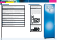

www.schaeferpower.de
Technical Notes Technical Notes
Basic Topologies
There are various circuit topologies and the selection depends on the requirements, such as low or high input voltage, low or high output
voltage, single or multi output, power rating. The following circuits present our common concepts of power conversion.
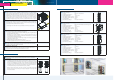
Push Pull Converter
The push pull converter is often used
for applications with low input voltage.
The switching transistors are alternately
conducting with variable pulse-width. At the
secondary side, after rectification and filtering,
the output voltage is sensed and compared
with a reference. The error signal controls via
an opto-coupler the primary circuit.
Half Bridge Converter
The following circuit shows, as an example, a
converter with dual AC input in a half bridge
connection. With the input voltage supplied
to the 230 V terminal, the rectifier circuit is a
standard bridge connection; supplied to the
115 V terminal the rectifier circuit functions as
a voltage doubler circuit.
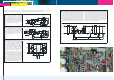
DC/AC Inverter
The diagram beside shows the circuit of an
inverter. The DC input voltage is transformed
by the power transistors T1-T4 with the parallel
connected inverse diodes D1-D4 in a pulse-
width modulated square wave voltage. The
choke with the windings LI and LII integrates
this voltage, and at the capacitor C a sinusoidal
output voltage is available. The power
transistors are controlled via opto-coupler in
such a way that not both transistors of one
branch are conducting at the same time. The
output voltage is sensed and compared with
a reference signal generating the firing pulses
for the power transistors. The output current
is measured via shunt R1 and limited through
the control circuit. Isolation between input
and output and voltage transformation can
either be provided by a converter connected
to the input of an inverter or by a transformer
connected to the output of an inverter.
output
sense
ripple
I-lim.
I-lim.
sec.controlprim.control
opto-
couplers
DC
filter
input
-
-
+
+
+
-
RFI
filter
OVP
main
output
sense
ripple
I-lim.
sec.control
filter
-
+
+
-
prim.control
opto-
couplers
RFI
filter
115V AC
230V AC
0V
AC input
OVP
- rect.
I-lim.
D1
D2
D3
D4
T1
T2
T4
T3
R2 LI LII
R1
C
control + PWM
current
voltage
sense
sense
opto-
coupler
opto-
coupler
Inverter AC out
p
ut
Inverter
DC input
Full Bridge Converter with Zero Voltage Switching (ZVS)
For the higher power modules presented from page 46 to 67
the primary circuit is performed as a full bridge connection
with four switching transistors (IGBTs) being controlled by the
driver and protective circuits. The special mode of driving the
IGBTs in conjunction with the resonant choke and the symmet-
rical capacitor allows for “zero voltage switching” which im-
proves the efficiency and reduces the switching noise. The in-
put can be designed for both, DC or AC. At the secondary side
of the transformer the voltage is rectified and filtered. Then the
output voltage is sensed and compared with a reference, and
the error signal controls via opto-coupler the switching transis-
tors on the primary side. For over voltage protection the OVP
circuit senses the output voltage and turns off the switching
transistors if a certain level is reached. The circuit automatically
returns to operation but is repeatedly switched off and turned
on again if the over voltage condition is still present. If the unit
does not return to normal operation within a short period of
time, it will then be switched off. For current limiting the signal
sensed by the LEM transformer starts to reduce the output volt-
age if the current exceeds a certain limit.
IGBTs
Driver
and protective
circuits for IGBTs
resonant
control
symmetrical
LEM
transformer
capacitor
ripple filter
opto-
coupler
OVP
+
-
sense
RFI filter
+
-
DC input
DC output
+
-
choke