
Datasheet


07-2018, Rev. 0718
www.te.com
© 2014 Tyco Electronics Corporation,
a TE Connectivity Ltd. company
Datasheets and product specification
according to IEC 61810-1 and to be used
only together with the ‘Definitions’ section.
Datasheets and product data is subject to the
terms of the disclaimer and all chapters of
the ‘Definitions’ section, available at
http://relays.te.com/definitions
Datasheets, product data, ‘Definitions’ sec-
tion, application notes and all specifications
are subject to change.
2
SCHRACK
General Purpose Relays
PCB Relays
Power PCB Relay RT1 (Continued)
Other Data (continued)
Terminal type
standard version PCB-THT, plug-in
reflow version PCB-THR
Mounting distance AC coil: ≥2.5mm
Weight 14g
Resistance to soldering heat THT, IEC 60068-2-20
RTII 270°C/10s
RTIII 260°C/5s
Resistance to soldering heat THR
reflow soldering (for reflow version) forced gas convection
4)
or
vapour phase
5)
temperature profile according EN61730
Packaging/unit tube/20 pcs., box/500 pcs.
4) infrared heating not allowed
5) recommended fluid LS/230
Accessories
For details see datasheet
Accessories Industrial Power Relay RT
NOTE: indicated contact ratings and electrical endurance data for direct
wiring of relays (according IEC 61810-1); for relays mounted on sockets
deratings may apply.
Insulation Data
Initial dielectric strength
between open contacts 1000V
rms
between contact and coil 5000V
rms
Clearance/creepage
between contact and coil ≥10/10mm
Material group of insulation parts IIIa
Tracking index of relay base PTI 250V
reflow version PTI 175V
Other Data
Material compliance: EU RoHS/ELV, China RoHS, REACH, Halogen content
refer to the Product Compliance Support Center at
www.te.com/customersupport/rohssupportcenter
Resistance to heat and fire
WG version or Reflow version according EN60335, par30
Ambient temperature
DC coil -40 to 85°C
AC coil -40 to 70°C
Category of environmental protection, IEC 61810
standard version RTII - flux proof, RTIII - wash tight
reflow version RTII - flux proof
Vibration resistance (functional)
form A/form B contact, 30 to 500Hz 20g/5g
Shock resistance (destructive) 100g
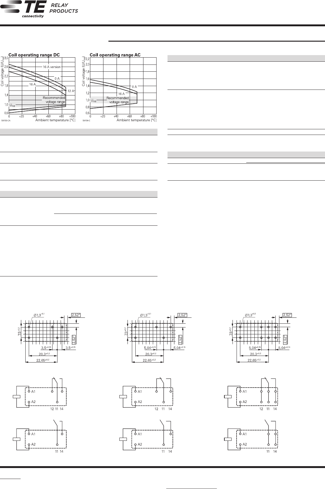
PCB layout / terminal assignment
Bottom view on solder pins
12 A, pinning 3.5 mm
1 form C (CO) contact
1 form A (NO) contact
12 A, pinning 5 mm
1 form C (CO) contact
1 form A (NO) contact
16 A, pinning 5 mm
1 form C (CO) contact
1 form A (NO) contact
S0418-CB S0418-CN S0418-CA
S0163-BES0163-BCS0163-BG
S0163-BH S0163-BD S0163-BF
*) With the recommended PCB hole sizes a grid
pattern from 2.5 mm to 2.54 mm can be used.