
Product manual
University of Hertfordshire
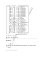
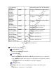
In this project Port A was used to transfer data, which was bidirectional. Port B was used to
control the control block on the IDE interface. Port C was used to control the two I/O chips.
5.5 IDE I/O Adapt Manufacture
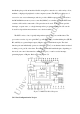
The details of pin connecting and function will be introduced here. However, a clearer
circuit diagram will be shown in Appendix D. The first 74HC245 was used to transfer data,
which is bidirectional. The second one was used to transfer the control signals, which is
unidirectional.
5.5.1 Data Block
At first the pins D0-D7 connected to A0-A7 on the first 74HC245 and the output of the chip
B0-B7 connected to the Port A of the MC68230. However, the D0-D7connected to A7-A0
and B7-B0 connected to PA0-PA7 after carefully consideration of the arrangement of the
circuit.
5.5.2 Control Block
As mentioned before PB0-PB7 respectively connected to CS1FX, CS3FX, DA2, DA1, DA0,
DIOR, DIOW to control I/O port functions and selection addressed of IDE on the hard disk.
PC0 and PC1 connected to two I/O chip OE- pin to enable two chips. PC1 connected to the
first chip DIR pin to control the direction of the data transfer.
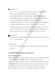
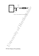
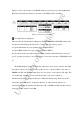
5.5.3 Reset Button
As introduced above this signal from the host system shall be asserted during power on and
negated thereafter unless some event requires that the drive(s) be reset following power on.
Thus a button switch was used to control the reset of the hard disk. A circuit diagram is
shown as below: