Atmel SAM D21E / SAM D21G / SAM D21J SMART ARM-Based Microcontroller DATASHEET Description The Atmel® | SMART™ SAM D21 is a series of low-power microcontrollers using the 32-bit ARM® Cortex®-M0+ processor, and ranging from 32- to 64-pins with up to 256KB Flash and 32KB of SRAM. The SAM D21 devices operate at a maximum frequency of 48MHz and reach 2.46 CoreMark/MHz.
Features z Processor z ARM Cortex-M0+ CPU running at up to 48MHz z Single-cycle hardware multiplier z Micro Trace Buffer (MTB) z Memories z 32/64/128/256KB in-system self-programmable Flash z 4/8/16/32KB SRAM Memory z System z Power-on reset (POR) and brown-out detection (BOD) z Internal and external clock options with 48MHz Digital Frequency Locked Loop (DFLL48M) and 48MHz to 96MHz Fractional Digital Phase Locked Loop (FDPLL96M) z External Interrupt Controller (EIC) z 16 external interrupts z One non-maska
1.
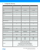
SAM D21J SAM D21G SAM D21E Event System channels 12 12 12 SW Debug Interface Yes Yes Yes Watchdog Timer (WDT) Yes Yes Yes Atmel | SMART SAM D21 [DATASHEET] Atmel-42181G–SAM-D21_Datasheet–09/2015 4
2.
2.1.
2.1.2 Device Variant B Ordering Code FLASH (bytes) SRAM (bytes) Package ATSAMD21E15B-AU Tray ATSAMD21E15B-AUT TQFP32 ATSAMD21E15B-AF ATSAMD21E15B-AFT ATSAMD21E15B-MU 32K QFN32 ATSAMD21E15B-MFT 32K 4K WLCSP35 TQFP32 ATSAMD21E16B-AF 64K QFN32 ATSAMD21E16B-MFT 2.2.
2.2.
2.2.
2.3.
2.3.
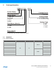
Block Diagram SWCLK CORTEX-M0+ PROCESSOR Fmax 48 MHz SERIAL WIRE SWDIO DEVICE SERVICE UNIT M MICRO TRACE BUFFER IOBUS 256/128/64/32KB NVM 32/16/8/4KB RAM NVM CONTROLLER Cache SRAM CONTROLLER M S S M HIGH SPEED BUS MATRIX PERIPHERAL ACCESS CONTROLLER S AHB-APB BRIDGE B S AHB-APB BRIDGE A DM SOF 1KHZ PERIPHERAL ACCESS CONTROLLER DMA 66xxSERCOM SERCOM VREF PAD0 PAD1 PAD2 PAD3 OSCULP32K OSC32K XIN32 XOUT32 DP AHB-APB BRIDGE C SYSTEM CONTROLLER BOD33 DMA USB FS DEVICE MINI-HOST
Pinout 4.1 SAM D21J 4.1.1 QFN64 / TQFP64 64 63 62 61 60 59 58 57 56 55 54 53 52 51 50 49 PB03 PB02 PB01 PB00 PB31 PB30 PA31 PA30 VDDIN VDDCORE GND PA28 RESETN PA27 PB23 PB22 4.
4.1.
SAM D21G 4.2.1 QFN48 / TQFP48 48 47 46 45 44 43 42 41 40 39 38 37 PB03 PB02 PA31 PA30 VDDIN VDDCORE GND PA28 RESETN PA27 PB23 PB22 4.
4.2.
SAM D21E 4.3.1 QFN32 / TQFP32 32 31 30 29 28 27 26 25 PA31 PA30 VDDIN VDDCORE GND PA28 RESETN PA27 4.
4.3.
5. Signal Descriptions List The following table gives details on signal names classified by peripheral.
Signal Name Function Type WO[1:0] Waveform Outputs Output Waveform Outputs Output Active Level Timer Counter - TCCx WO[1:0] Peripheral Touch Controller - PTC X[15:0] PTC Input Analog Y[15:0] PTC Input Analog General Purpose I/O - PORT PA25 - PA00 Parallel I/O Controller I/O Port A I/O PA28 - PA27 Parallel I/O Controller I/O Port A I/O PA31 - PA30 Parallel I/O Controller I/O Port A I/O PB17 - PB00 Parallel I/O Controller I/O Port B I/O PB23 - PB22 Parallel I/O Controller I/O Port
6. I/O Multiplexing and Considerations 6.1 Multiplexed Signals Each pin is by default controlled by the PORT as a general purpose I/O and alternatively it can be assigned to one of the peripheral functions A, B, C, D, E, F, G or H. To enable a peripheral function on a pin, the Peripheral Multiplexer Enable bit in the Pin Configuration register corresponding to that pin (PINCFGn.PMUXEN, n = 0-31) in the PORT must be written to one.
Table 6-1.
Table 6-1.
6.2 Other Functions 6.2.1 Oscillator Pinout The oscillators are not mapped to the normal PORT functions and their multiplexing are controlled by registers in the System Controller (SYSCTRL). 6.2.2 Oscillator Supply XOSC VDDIO XOSC32K VDDANA Signal I/O Pin XIN PA14 XOUT PA15 XIN32 PA00 XOUT32 PA01 Serial Wire Debug Interface Pinout Only the SWCLK pin is mapped to the normal PORT functions.
ADC PA[7:2] VDDIO VDDIN GND Power Domain Overview VDDCORE 7.1 GNDANA Power Supply and Start-Up Considerations VDDANA 7. VOLTAGE REGULATOR PB[31:10] OSC8M PA[13:8] BOD12 XOSC AC PB[9:0] PA[15:14] PA[31:16] DAC PTC Digital Logic (CPU, peripherals) PA[1:0] XOSC32K POR DFLL48M OSC32K OSCULP32K 7.2 Power Supply Considerations 7.2.1 Power Supplies BOD33 FDPLL96M The Atmel® SAM D21 has several different power supply pins: z VDDIO: Powers I/O lines, OSC8M and XOSC. Voltage is 1.
The ground pins, GND, are common to VDDCORE, VDDIO and VDDIN. The ground pin for VDDANA is GNDANA. For decoupling recommendations for the different power supplies, refer to the schematic checklist. Refer to “Schematic Checklist” on page 1008 for details. 7.2.2 Voltage Regulator The SAM D21 voltage regulator has two different modes: 7.2.3 z Normal mode: To be used when the CPU and peripherals are running z Low Power (LP) mode: To be used when the regulator draws small static current.
7.3 Power-Up This section summarizes the power-up sequence of the SAM D21. The behavior after power-up is controlled by the Power Manager. Refer to “PM – Power Manager” on page 117 for details. 7.3.1 Starting of Clocks After power-up, the device is set to its initial state and kept in reset, until the power has stabilized throughout the device. Once the power has stabilized, the device will use a 1MHz clock.
8. Product Mapping Figure 8-1.
9. Memories 9.1 Embedded Memories 9.2 z Internal high-speed flash with Read-While-Write (RWW) capability on section of the array (Device Variant B). z Internal high-speed flash z Internal high-speed RAM, single-cycle access at full speed Physical Memory Map The High-Speed bus is implemented as a bus matrix. All High-Speed bus addresses are fixed, and they are never remapped in any way, even during boot.
9.3 NVM Calibration and Auxiliary Space The device calibration data are stored in different sections of the NVM calibration and auxiliary space presented in Figure 9-1. Figure 9-1.
Table 9-4. 9.3.2 NVM User Row Mapping Bit Position Name Usage 2:0 BOOTPROT 3 Reserved 6:4 EEPROM 7 Reserved 13:8 BOD33 Level BOD33 Threshold Level at power on. Refer to BOD33 register. Default value = 7. 14 BOD33 Enable BOD33 Enable at power on . Refer to BOD33 register. Default value = 1. 16:15 BOD33 Action BOD33 Action at power on. Refer to BOD33 register. Default value = 1. 24:17 Reserved 25 WDT Enable WDT Enable at power on. Refer to WDT CTRL register. Default value = 0.
Table 9-5. 9.3.3 NVM Software Calibration Area Mapping Bit Position Name Description 2:0 Reserved 14:3 Reserved 26:15 Reserved 34:27 ADC LINEARITY ADC Linearity Calibration. Should be written to CALIB register. 37:35 ADC BIASCAL ADC Bias Calibration. Should be written to CALIB register. 44:38 OSC32K CAL OSC32KCalibration. Should be written to OSC32K register. 49:45 USB TRANSN USB TRANSN calibration value. Should be written to PADCAL register.
10. Processor And Architecture 10.1 Cortex M0+ Processor The Atmel | SMART SAM D21 implements the ARM® Cortex™-M0+ processor, based on the ARMv6 Architecture and Thumb®-2 ISA. The Cortex M0+ is 100% instruction set compatible with its predecessor, the Cortex-M0 core, and upward compatible to Cortex-M3 and M4 cores. The ARM Cortex-M0+ implemented is revision r0p1. For more information refer to www.arm.com. 10.1.1 Cortex M0+ Configuration Table 10-1.
z Nested Vectored Interrupt Controller (NVIC) z z System Control Block (SCB) z z External interrupt signals connect to the NVIC, and the NVIC prioritizes the interrupts. Software can set the priority of each interrupt. The NVIC and the Cortex-M0+ processor core are closely coupled, providing low latency interrupt processing and efficient processing of late arriving interrupts. Refer to “Nested Vector Interrupt Controller” on page 34 and the Cortex-M0+ Technical Reference Manual for details (www.arm.
writing a one to the corresponding bit in the peripheral’s Interrupt Enable Clear (INTENCLR) register. An interrupt request is generated from the peripheral when the interrupt flag is set and the corresponding interrupt is enabled. The interrupt requests for one peripheral are ORed together on system level, generating one interrupt request for each peripheral. An interrupt request will set the corresponding interrupt pending bit in the NVIC interrupt pending registers (SETPEND/CLRPEND bits in ISPR/ICPR).
Table 10-3. Interrupt Line Mapping (Continued) Peripheral Source 10.3 NVIC Line TC3 – Timer Counter 3 18 TC4 – Timer Counter 4 19 TC5 – Timer Counter 5 20 TC6 – Timer Counter 6 21 TC7 – Timer Counter 7 22 ADC – Analog-to-Digital Converter 23 AC – Analog Comparator 24 DAC – Digital-to-Analog Converter 25 PTC – Peripheral Touch Controller 26 I2S - Inter IC Sound 27 Micro Trace Buffer 10.3.
z POSITION: Contains the trace write pointer and the wrap bit, z MASTER: Contains the main trace enable bit and other trace control fields, z FLOW: Contains the WATERMARK address and the AUTOSTOP and AUTOHALT control bits, z BASE: Indicates where the SRAM is located in the processor memory map. This register is provided to enable auto discovery of the MTB SRAM location, by a debug agent. See the CoreSight MTB-M0+ Technical Reference Manual for a detailed description of these registers. 10.
10.4.2 Configuration Priviledged SRAM-access MASTERS Multi-Slave MASTERS CM0+ 0 DSU DSU 1 DMACDSU Data 2 DMAC Data DSU MASTER ID CM0+ 3 DMAC Fetch AHB-APB Bridge C 2 DMAC WB AHB-APB Bridge B 1 USB AHB-APB Bridge A 0 SRAM MTB Internal Flash High-Speed Bus SLAVES 0 1 2 3 4 4 5 5 6 6 SLAVE ID SRAM PORT ID MTB USB DMAC WB DMAC Fetch Table 10-4.
Table 10-6. SRAM Port Connection SRAM Port Connection Port ID Connection Type MTB - Micro Trace Buffer 0 Direct USB - Universal Serial Bus 1 Direct DMAC - Direct Memory Access Controller - Write-Back Access 2 Direct DMAC - Direct Memory Access Controller - Fetch Access 3 Direct CM0+ - Cortex M0+ Processor 4 Bus Matrix DMAC - Direct Memory Access Controller - Data Access 5 Bus Matrix DSU - Device Service Unit 6 Bus Matrix 10.4.
10.5 AHB-APB Bridge The AHB-APB bridge is an AHB slave, providing an interface between the high-speed AHB domain and the low-power APB domain. It is used to provide access to the programmable control registers of peripherals (see “Product Mapping” on page 28). AHB-APB bridge is based on AMBA APB Protocol Specification V2.0 (ref.
Figure 10-2. APB Read Access. T0 T1 T2 T3 T0 PCLK PADDR Addr 1 PADDR PWRITE PSEL PSEL PENABLE PENABLE Data 1 PREADY T3 T4 T5 Addr 1 PRDATA Data 1 PREADY No wait states 10.6 T2 PCLK PWRITE PRDATA T1 Wait states PAC – Peripheral Access Controller 10.6.1 Overview There is one PAC associated with each AHB-APB bridge. The PAC can provide write protection for registers of each peripheral connected on the same bridge.
10.6.2 Register Description Atomic 8-, 16- and 32-bit accesses are supported. In addition, the 8-bit quarters and 16-bit halves of a 32-bit register, and the 8-bit halves of a 16-bit register can be accessed directly. Refer to “Product Mapping” on page 28 for PAC locations. 10.6.2.
Write Protect Set Name: WPSET Offset: 0x04 Reset: 0x00000000 Property: - Bit 31 30 29 28 27 26 25 24 Access R R R R R R R R Reset 0 0 0 0 0 0 0 0 Bit 23 22 21 20 19 18 17 16 Access R R R R R R R R Reset 0 0 0 0 0 0 0 0 Bit 15 14 13 12 11 10 9 8 Access R R R R R R R R Reset 0 0 0 0 0 0 0 0 Bit 7 6 5 4 3 2 1 0 EIC RTC WDT GCLK SYSCTRL PM Access R R/W R/W R/W R/W R/W R/W R Reset 0 0 0 0 0 0 0
10.6.2.
Write Protect Set Name: WPSET Offset: 0x04 Reset: 0x00000002 Property: - Bit 31 30 29 28 27 26 25 24 Access R R R R R R R R Reset 0 0 0 0 0 0 0 0 Bit 23 22 21 20 19 18 17 16 Access R R R R R R R R Reset 0 0 0 0 0 0 0 0 Bit 15 14 13 12 11 10 9 8 Access R R R R R R R R Reset 0 0 0 0 0 0 0 0 Bit 7 6 5 4 3 2 1 0 MTB USB DMAC PORT NVMCTRL DSU Access R R/W R/W R/W R/W R/W R/W R Reset 0 0 0 0 0 0
10.6.2.
Write Protect Set Name: WPSET Offset: 0x04 Reset: 0x00800000 Property: - Bit 31 30 29 28 27 26 25 24 Access R R R R R R R R Reset 0 0 0 0 0 0 0 0 Bit 23 22 21 20 19 18 17 16 AC1 I2S PTC DAC AC ADC Access R R R/W R/W R/W R/W R/W R/W Reset 1 0 0 0 0 0 0 0 Bit 15 14 13 12 11 10 9 8 TC7 TC6 TC5 TC4 TC3 TCC2 TCC1 TCC0 R/W R/W R/W R/W R/W R/W R/W R/W Reset 0 0 0 0 0 0 0 0 Bit 7 6 5 4 3 2 1 0 SERCOM5 SER
11. Peripherals Configuration Summary Table 11-1.
Table 11-1.
12. DSU – Device Service Unit 12.1 Overview The Device Service Unit (DSU) provides a means to detect debugger probes. This enables the ARM Debug Access Port (DAP) to have control over multiplexed debug pads and CPU reset. The DSU also provides system-level services to debug adapters in an ARM debug system. It implements a CoreSight Debug ROM that provides device identification as well as identification of other debug components in the system.
12.4 Signal Description Signal Name Type Description RESET Digital Input External reset SWCLK Digital Input SW clock SWDIO Digital I/O SW bidirectional data pin Refer to “I/O Multiplexing and Considerations” on page 21 for details on the pin mapping for this peripheral. 12.5 Product Dependencies In order to use this peripheral, other parts of the system must be configured correctly, as described below. 12.5.
12.5.8 Analog Connections Not applicable. 12.6 Debug Operation 12.6.1 Principle of Operation The DSU provides basic services to allow on-chip debug using the ARM Debug Access Port and the ARM processor debug resources: z CPU reset extension z Debugger probe detection For more details on the ARM debug components, refer to the ARM Debug Interface v5Architecture Specification. 12.6.
reset or external reset occurs. Availability of the Hot-Plugging feature can be read from the Hot-Plugging Enable bit of the Status B register (STATUSB.HPE). Figure 12-3. Hot-Plugging Detection Timing Diagram SWCLK RESET CPU_STATE reset running Hot-Plugging The presence of a debugger probe is detected when either Hot-Plugging or Cold-Plugging is detected. Once detected, the Debugger Present bit of the Status B register (STATUSB.DBGPRES) is set.
12.9 1. At power up, RESET is driven low by a debugger. The on-chip regulator holds the system in a POR state until the input supply is above the POR threshold (refer to “Power-On Reset (POR) Characteristics” on page 952). The system continues to be held in this static state until the internally regulated supplies have reached a safe operating state. 2. The PM starts, clocks are switched to the slow clock (Core Clock, System Clock, Flash Clock and any Bus Clocks that do not have clock gate control).
Figure 12-4. APB Memory Mapping 0x0000 DSU operating registers 0x00FC 0x0100 0x01FD Internal address range (cannot be accessed from debug tools when the device is protected by the NVMCTRL security bit) Replicated DSU operating registers Empty External address range (can be accessed from debug tools with some restrictions) 0x1000 DSU CoreSight ROM 0x1FFC Some features not activated by APB transactions are not available when the device is protected: Table 12-1.
Table 12-2. Conceptual 64-Bit Peripheral ID Bit Descriptions Field Size JEP-106 CC code 4 Atmel continuation code: 0x0 JEP-106 ID code 7 Atmel device ID: 0x1F 4KB count 4 Indicates that the CoreSight component is a ROM: 0x0 PID4 RevAnd 4 Not used; read as 0 PID3 CUSMOD 4 Not used; read as 0 PID3 PARTNUM 12 Contains 0xCD0 to indicate that DSU is present 4 DSU revision (starts at 0x0 and increments by 1 at both major and minor revisions). Identifies DSU identification method variants.
12.11.3 32-bit Cyclic Redundancy Check (CRC32) The DSU unit provides support for calculating a cyclic redundancy check (CRC32) value for a memory area (including flash and AHB RAM). When the CRC32 command is issued from: z The internal range, the CRC32 can be operated at any memory location z The external range, the CRC32 operation is restricted; DATA, ADDR and LENGTH values are forced (see below) Table 12-3.
read. The DCC0 and DCC1 registers are shared with the onboard memory testing logic (MBIST). Accordingly, DCC0 and DCC1 must not be used while performing MBIST operations. 12.11.5 Testing of Onboard Memories (MBIST) The DSU implements a feature for automatic testing of memory also known as MBIST. This is primarily intended for production test of onboard memories.
z ADDR: Address of the word containing the failing bit. z DATA: contains data to identify which bit failed, and during which phase of the test it failed. The DATA register will in this case contains the following bit groups: Table 12-4.
Table 12-6. Available Features When Operated From The External Address Range and Device is Protected Availability From The External Address Range and Device is Protected Features Chip-Erase command and status CRC32 Yes Yes, only full array or full EEPROM CoreSight Compliant Device identification Yes Debug communication channels Yes Testing of onboard memories (MBIST) Yes STATUSA.CRSTEXT clearing No (STATUSA.
12.12 Register Summary Table 12-7. Register Summary Offset Name Bit Pos.
Offset Name 0x1004 0x1005 Bit Pos. 7:0 ENTRY1 15:8 FMT ADDOFF[3:0] 0x1006 23:16 ADDOFF[11:4] 0x1007 31:24 ADDOFF[19:12] 0x1008 7:0 END[7:0] 0x1009 0x100A END 0x100B 0x100C ...
Offset Name Bit Pos.
12.13 Register Description Registers can be 8, 16 or 32 bits wide. Atomic 8-, 16- and 32-bit accesses are supported. In addition, the 8-bit quarters and 16-bit halves of a 32-bit register and the 8-bit halves of a 16-bit register can be accessed directly. Some registers are optionally write-protected by the Peripheral Access Controller (PAC). Write protection is denoted by the Write-Protected property in each individual register description. Refer to “Register Access Protection” on page 51 for details.
12.13.1 Control Name: CTRL Offset: 0x0000 Reset: 0x00 Property: Write-Protected Bit 7 6 5 4 3 2 CE MBIST CRC 1 0 SWRST Access R R R W W W R W Reset 0 0 0 0 0 0 0 0 z Bits 7:5 – Reserved These bits are unused and reserved for future use. For compatibility with future devices, always write these bits to zero when this register is written. These bits will always return zero when read. z Bit 4 – CE: Chip Erase Writing a zero to this bit has no effect.
12.13.2 Status A Name: STATUSA Offset: 0x0001 Reset: 0x00 Property: Write-Protected Bit 7 6 5 4 3 2 1 0 PERR FAIL BERR CRSTEXT DONE Access R R R R/W R/W R/W R/W R/W Reset 0 0 0 0 0 0 0 0 z Bits 7:5 – Reserved These bits are unused and reserved for future use. For compatibility with future devices, always write these bits to zero when this register is written. These bits will always return zero when read.
12.13.3 Status B Name: STATUSB Offset: 0x0002 Reset: 0x1X Property: Write-Protected Bit 7 6 5 4 3 2 1 0 HPE DCCD1 DCCD0 DBGPRES PROT Access R R R R R R R R Reset 0 0 0 1 0 0 X X z Bits 7:5 – Reserved These bits are unused and reserved for future use. For compatibility with future devices, always write these bits to zero when this register is written. These bits will always return zero when read.
12.13.
12.13.
12.13.
12.13.7 Debug Communication Channel n Name: DCCn Offset: 0x0010+n*0x4 [n=0..
12.13.8 Device Identification The information in this register is related to the ordering code. Refer to the “Ordering Information” on page 5 for details.
z Bits 11:8 – REVISION[3:0]: Revision Identifies the die revision number. z Bits 7:0 – DEVSEL[7:0]: Device Select DEVSEL is used to identify a device within a product family and product series. The value corresponds to the Flash memory density, pin count and device variant parts of the ordering code. Refer to “Ordering Information” on page 5 for details. Table 12-8.
12.13.9 Coresight ROM Table Entry n Name: ENTRYn Offset: 0x1000+n*0x4 [n=0..
12.13.
12.13.
12.13.
12.13.
12.13.
12.13.
12.13.
12.13.
12.13.
12.13.
12.13.
Atmel | SMART SAM D21 [DATASHEET] Atmel-42181G–SAM-D21_Datasheet–09/2015 86
13. Clock System This chapter only aims to summarize the clock distribution and terminology in the SAM D21 device. It will not explain every detail of its configuration. For in-depth documentation, see the referenced module chapters. 13.1 Clock Distribution Figure 13-1.
Figure 13-2. Example of SERCOM clock PM Synchronous Clock Controller SYSCTRL DFLL48M 13.2 CLK_SERCOM0_APB GCLK Generic Clock Generator 1 Generic Clock Multiplexer 20 GCLK_SERCOM0_CORE SERCOM 0 Synchronous and Asynchronous Clocks As the CPU and the peripherals can be clocked from different clock sources, possibly with widely different clock speeds, some peripheral accesses by the CPU needs to be synchronized between the different clock domains.
Figure 13-3. Synchronization Asynchronous Domain (generic clock) Synchronous Domain (CLK_APB) Sync Non Synced reg Peripheral bus INTFLAG Write-Synced reg SYNCBUSY STATUS READREQ Synchronizer Write-Synced reg R/W-Synced reg 13.3.1.2 Write-Synchronization The write-synchronization is triggered by a write to any generic clock core register. The Synchronization Busy bit in the Status register (STATUS.
13.3.1.3 Read-Synchronization Reading a read-synchronized core register will cause the peripheral bus to stall immediately until the readsynchronization is complete. STATUS.SYNCBUSY will not be set. Refer to “Synchronization Delay” on page 91 for details on the synchronization delay. Note that reading a read-synchronized core register while STATUS.
CTRL.SWRST bit has no effect. The Synchronisation Ready interrupt (if available) cannot be used for Software Reset write-synchronization. When the software reset is in progress (STATUS.SYNCBUSY and CTRL.
When user makes a 32-bit access to offset 0x00, all registers are written but REGA, REGB, REGC can be updated at a different time because of independent write synchronization 13.3.2.3 General read synchronization Before any read of a core register, the user must check that the related bit in SYNCBUSY register is cleared. Read access to core register is always immediate but the return value is reliable only if a synchonization of this core register is not going. 13.3.2.
13.5 On-demand, Clock Requests Figure 13-4. Clock request routing Clock request DFLL48M Generic Clock Generator ENABLE GENEN RUNSTDBY RUNSTDBY Clock request Generic Clock Multiplexer Clock request Peripheral CLKEN ENABLE RUNSTDBY ONDEMAND All the clock sources in the system can be run in an on-demand mode, where the clock source is in a stopped state when no peripherals are requesting the clock source. Clock requests propagate from the peripheral, via the GCLK, to the clock source.
z All generic clocks disabled except: z the WDT generic clock using the generator 2 as source On a user reset the GCLK starts to their initial state, except for: z generic clocks that are write-locked (WRTLOCK is written to one prior to reset or the WDT generic clock if the WDT Always-On at power on bit set in the NVM User Row) z The generic clock dedicated to the RTC if the RTC generic clock is enabled On any reset the clock sources are reset to their initial state except the 32KHz clock sources whi
14. GCLK – Generic Clock Controller 14.1 Overview Several peripherals may require specific clock frequencies to operate correctly. The Generic Clock Controller consists of number of generic clock generators and generic clock multiplexers that can provide a wide range of clock frequencies. The generic clock generators can be set to use different external and internal clock sources. The selected clock can be divided down in the generic clock generator.
Figure 14-2.
14.5.4 DMA Not applicable. 14.5.5 Interrupts Not applicable. 14.5.6 Events Not applicable. 14.5.7 Debug Operation Not applicable. 14.5.8 Register Access Protection All registers with write-access are optionally write-protected by the Peripheral Access Controller (PAC). Write-protection is denoted by the Write-Protection property in the register description. When the CPU is halted in debug mode or the CPU reset is extended, all write-protection is automatically disabled.
Refer to GENCTRL register for details. 3. The generic clock must be configured by performing a single 16-bit write to the Generic Clock Control register (CLKCTRL): z The generic clock that will be configured must be written to the ID bit group (CLKCTRL.ID) z The generic clock generator used as the source of the generic clock must be written to the GEN bit group (CLKCTRL.GEN) Refer to CLKCTRL register for details. 14.6.2.
14.6.2.6 Selecting a Clock Source for the Generic Clock Generator Each generic clock generator can individually select a clock source by writing to the Source Select bit group in GENCTRL (GENCTRL.SRC). Changing from one clock source, A, to another clock source, B, can be done on the fly. If clock source B is not ready, the generic clock generator will continue running with clock source A. As soon as clock source B is ready, however, the generic clock generator will switch to it.
When a generic clock generator has been selected, the generic clock is enabled by writing a one to the Clock Enable bit in CLKCTRL (CLKCTRL.CLKEN). The CLKCTRL.CLKEN bit must be synchronized to the generic clock domain. CLKCTRL.CLKEN will continue to read as its previous state until the synchronization is complete. 14.6.3.2 Disabling a Generic Clock A generic clock is disabled by writing a zero to CLKCTRL.CLKEN. The SYNCBUSY bit will be cleared when this writesynchronization is complete. CLKCTRL.
For example, the sequence to read the GENCTRL register of generic clock generator i is: 1. Do an 8-bit write of the i value to GENCTRL.ID 2. Read GENCTRL 14.6.4.2 Generic Clock Enable after Reset The Generic Clock Controller must be able to provide a generic clock to some specific peripherals after a reset. That means that the configuration of the generic clock generators and generic clocks after reset is device-dependent. Refer to Table 14-9 and Table 14-10 for details on GENCTRL reset.
14.7 Register Summary Table 14-2. Register Summary Offset Name Bit Pos.
14.8 Register Description Registers can be 8, 16 or 32 bits wide. Atomic 8-, 16- and 32-bit accesses are supported. In addition, the 8-bit quarters and 16-bit halves of a 32-bit register and the 8-bit halves of a 16-bit register can be accessed directly. Some registers are optionally write-protected by the Peripheral Access Controller (PAC). Write-protection is denoted by the Write-protected property in each individual register description. Refer to “Register Access Protection” on page 97 for details.
14.8.1 Control Name: CTRL Offset: 0x0 Reset: 0x00 Property: Write-Protected, Write-Synchronized Bit 7 6 5 4 3 2 1 0 SWRST Access R R R R R R R R/W Reset 0 0 0 0 0 0 0 0 z Bits 7:1 – Reserved These bits are unused and reserved for future use. For compatibility with future devices, always write these bits to zero when this register is written. These bits will always return zero when read. z Bit 0 – SWRST: Software Reset 0: There is no reset operation ongoing.
14.8.2 Status Name: STATUS Offset: 0x1 Reset: 0x00 Property: - Bit 7 6 5 4 3 2 1 0 SYNCBUSY Access R R R R R R R R Reset 0 0 0 0 0 0 0 0 z Bit 7 – SYNCBUSY: Synchronization Busy Status This bit is cleared when the synchronization of registers between the clock domains is complete. This bit is set when the synchronization of registers between clock domains is started. z Bits 6:0 – Reserved These bits are unused and reserved for future use.
14.8.3 Generic Clock Control This register allows the user to configure one of the generic clocks, as specified in the CLKCTRL.ID bit group. To write to the CLKCTRL register, do a 16-bit write with all configurations and the ID. To read the CLKCTRL register, first do an 8-bit write to the CLKCTRL.ID bit group with the ID of the generic clock whose configuration is to be read, and then read the CLKCTRL register.
Table 14-3. Generic Clock Generator (Continued) GEN[3:0] Name Description 0x4 GCLKGEN4 Generic clock generator 4 0x5 GCLKGEN5 Generic clock generator 5 0x6 GCLKGEN6 Generic clock generator 6 0x7 GCLKGEN7 Generic clock generator 7 0x8 GCLKGEN8 Generic clock generator 8 0x9-0xF Reserved z Bits 7:6 – Reserved These bits are unused and reserved for future use. For compatibility with future devices, always write these bits to zero when this register is written.
Table 14-4.
After a user reset, the reset value of the CLKCTRL register versus module instance is as shown in Table 14-6. Table 14-6. CLKCTRL Reset Value after a User Reset Module Instance Reset Value after a User Reset CLKCTRL.GEN CLCTRL.CLKEN CLKCTRL.
14.8.4 Generic Clock Generator Control This register allows the user to configure one of the generic clock generators, as specified in the GENCTRL.ID bit group. To write to the GENCTRL register, do a 32-bit write with all configurations and the ID. To read the GENCTRL register, first do an 8-bit write to the GENCTRL.ID bit group with the ID of the generic clock generator whose configuration is to be read, and then read the GENCTRL register.
z Bit 20 – DIVSEL: Divide Selection This bit is used to decide how the clock source used by the generic clock generator will be divided. If the clock source should not be divided, the DIVSEL bit must be zero and the GENDIV.DIV value for the corresponding generic clock generator must be zero or one. 0: The generic clock generator equals the clock source divided by GENDIV.DIV. 1: The generic clock generator equals the clock source divided by 2^(GENDIV.DIV+1).
Table 14-7.
Table 14-9. GENCTRL Reset Value after a Power Reset GCLK Generator ID Reset Value after a Power Reset 0x00 0x00010600 0x01 0x00000001 0x02 0x00010302 0x03 0x00000003 0x04 0x00000004 0x05 0x00000005 0x06 0x00000006 0x07 0x00000007 0x08 0x00000008 After a user reset, the reset value of the GENCTRL register is as shown in Table 14-10. Table 14-10.
14.8.5 Generic Clock Generator Division This register allows the user to configure one of the generic clock generators, as specified in the GENDIV.ID bit group. To write to the GENDIV register, do a 32-bit write with all configurations and the ID. To read the GENDIV register, first do an 8-bit write to the GENDIV.ID bit group with the ID of the generic clock generator whose configuration is to be read, and then read the GENDIV register.
Table 14-11. Division Factor Generator Division Factor Bits Generic clock generator 0 8 division factor bits - DIV[7:0] Generic clock generator 1 16 division factor bits - DIV[15:0] Generic clock generators 2 5 division factor bits - DIV[4:0] Generic clock generators 3 - 8 8 division factor bits - DIV[7:0] z Bits 7:4 – Reserved These bits are unused and reserved for future use. For compatibility with future devices, always write these bits to zero when this register is written.
Table 14-13. GENDIV Reset value after a Power Reset GCLK Generator ID Reset Value after a Power Reset 0x00 0x00000000 0x01 0x00000001 0x02 0x00000002 0x03 0x00000003 0x04 0x00000004 0x05 0x00000005 0x06 0x00000006 0x07 0x00000007 0x08 0x00000008 After a user reset, the reset value of the GENDIV register is as shown in Table 14-14. Table 14-14.
15. 15.1 PM – Power Manager Overview The Power Manager (PM) controls the reset, clock generation and sleep modes of the microcontroller. Utilizing a main clock chosen from a large number of clock sources from the GCLK, the clock controller provides synchronous system clocks to the CPU and the modules connected to the AHB and the APBx bus. The synchronous system clocks are divided into a number of clock domains; one for the CPU and AHB and one for each APBx.
15.3 Block Diagram Figure 15-1. PM Block Diagram POWER MANAGER CLK_APB GCLK SYNCHRONOUS CLOCK CONTROLLER CLK_AHB PERIPHERALS CLK_CPU SLEEP MODE CONTROLLER CPU BOD12 USER RESET BOD33 POWER RESET POR WDT RESET CONTROLLER CPU RESET RESET SOURCES 15.4 Signal Description Signal Name Type Description RESET Digital input External reset Refer to “I/O Multiplexing and Considerations” on page 21 for details on the pin mapping for this peripheral. One signal can be mapped on several pins. 15.
15.5.3 Clocks The PM bus clock (CLK_PM_APB) can be enabled and disabled in the power manager, and the default state of CLK_PM_APB can be found in Table 15-1. If this clock is disabled in the Power Manager, it can only be re-enabled by a reset. A generic clock (GCLK_MAIN) is required to generate the main clock. The clock source for GCLK_MAIN is configured by default in the Generic Clock Controller, and can be re-configured by the user if needed.
15.5.9 Analog Connections Not applicable. 15.6 Functional Description 15.6.1 Principle of Operation 15.6.1.1 Synchronous Clocks The GCLK_MAIN clock from GCLK module provides the source for the main clock, which is the common root for the synchronous clocks for the CPU and APBx modules. The main clock is divided by an 8-bit prescaler, and each of the derived clocks can run from any tapping off this prescaler or the undivided main clock, as long as fCPU ≥ fAPBx.
Similarly, the clock for the APBx can be divided by writing their respective registers (APBxSEL.APBxDIV). To ensure correct operation, frequencies must be selected so that fCPU ≥ fAPBx. Also, frequencies must never exceed the specified maximum frequency for each clock domain. Note that the AHB clock is always equal to the CPU clock. CPUSEL and APBxSEL can be written without halting or disabling peripheral modules.
Table 15-1.
There are two groups of reset sources: z Power Reset: Resets caused by an electrical issue. z User Reset: Resets caused by the application. The table below lists the parts of the device that are reset, depending on the reset type. Table 15-2.
Figure 15-3. Reset Controller RESET CONTROLLER BOD12 BOD33 POR RTC 32kHz clock sources WDT with ALWAYSON Generic Clock with WRTLOCK Debug Logic RESET WDT Others CPU RCAUSE RESET SOURCES 15.6.2.8 Sleep Mode Controller Sleep mode is activated by the Wait For Interrupt instruction (WFI). The Idle bits in the Sleep Mode register (SLEEP.IDLE) and the SLEEPDEEP bit of the System Control register of the CPU should be used as argument to select the level of the sleep mode.
Table 15-4.
15.6.3 SleepWalking SleepWalking is the capability for a device to temporarily wakeup clocks for peripheral to perform a task without wakingup the CPU in STANDBY sleep mode. At the end of the sleepwalking task, the device can either be waken-up by an interrupt (from a peripheral involved in SleepWalking) or enter again into STANDBY sleep mode. In Atmel | SMART SAM D21 devices, SleepWalking is supported only on GCLK clocks by using the on-demand clock principle of the clock sources.
15.7 Register Summary Table 15-5. Register Summary Offset Name Bit Pos. 0x00 CTRL 7:0 0x01 SLEEP 7:0 0x02 ... 0x07 Reserved 0x08 CPUSEL 7:0 CPUDIV[2:0] IDLE[1:0] 0x09 APBASEL 7:0 APBADIV[2:0] 0x0A APBBSEL 7:0 APBBDIV[2:0] 0x0B APBCSEL 7:0 APBCDIV[2:0] 0x0C ...
15.8 Register Description Registers can be 8, 16 or 32 bits wide. Atomic 8-, 16- and 32-bit accesses are supported. In addition, the 8-bit quarters and 16-bit halves of a 32-bit register, and the 8-bit halves of a 16-bit register can be accessed directly. Exception for APBASEL, APBBSEL and APBCSEL: These registers must only be accessed with 8-bit access. Some registers are optionally write-protected by the Peripheral Access Controller (PAC).
15.8.1 Control Name: CTRL Offset: 0x00 Reset: 0x00 Property: Write-Protected Bit 7 6 5 4 3 2 1 0 Access R R R R R R R R Reset 0 0 0 0 0 0 0 0 z Bits 7:0 – Reserved These bits are unused and reserved for future use. For compatibility with future devices, always write these bits to zero when this register is written. These bits will always return zero when read.
15.8.2 Sleep Mode Name: SLEEP Offset: 0x01 Reset: 0x00 Property: Write-Protected Bit 7 6 5 4 3 2 1 0 IDLE[1:0] Access R R R R R R R/W R/W Reset 0 0 0 0 0 0 0 0 z Bits 7:2 – Reserved These bits are unused and reserved for future use. For compatibility with future devices, always write these bits to zero when this register is written. These bits will always return zero when read.
15.8.3 CPU Clock Select Name: CPUSEL Offset: 0x08 Reset: 0x00 Property: Write-Protected Bit 7 6 5 4 3 2 1 0 CPUDIV[2:0] Access R R R R R R/W R/W R/W Reset 0 0 0 0 0 0 0 0 z Bits 7:3 – Reserved These bits are unused and reserved for future use. For compatibility with future devices, always write these bits to zero when this register is written. These bits will always return zero when read.
15.8.4 APBA Clock Select Name: APBASEL Offset: 0x09 Reset: 0x00 Property: Write-Protected Bit 7 6 5 4 3 2 1 0 APBADIV[2:0] Access R R R R R R/W R/W R/W Reset 0 0 0 0 0 0 0 0 z Bits 7:3 – Reserved These bits are unused and reserved for future use. For compatibility with future devices, always write these bits to zero when this register is written. These bits will always return zero when read.
15.8.5 APBB Clock Select Name: APBBSEL Offset: 0x0A Reset: 0x00 Property: Write-Protected Bit 7 6 5 4 3 2 1 0 APBBDIV[2:0] Access R R R R R R/W R/W R/W Reset 0 0 0 0 0 0 0 0 z Bits 7:3 – Reserved These bits are unused and reserved for future use. For compatibility with future devices, always write these bits to zero when this register is written. These bits will always return zero when read.
15.8.6 APBC Clock Select Name: APBCSEL Offset: 0x0B Reset: 0x00 Property: Write-Protected Bit 7 6 5 4 3 2 1 0 APBCDIV[2:0] Access R R R R R R/W R/W R/W Reset 0 0 0 0 0 0 0 0 z Bits 7:3 – Reserved These bits are unused and reserved for future use. For compatibility with future devices, always write these bits to zero when this register is written. These bits will always return zero when read.
15.8.
z Bit 2 – HPB2: HPB2 AHB Clock Mask 0: The AHB clock for the HPB2 is stopped. 1: The AHB clock for the HPB2 is enabled. z Bit 1 – HPB1: HPB1 AHB Clock Mask 0: The AHB clock for the HPB1 is stopped. 1: The AHB clock for the HPB1 is enabled. z Bit 0 – HPB0: HPB0 AHB Clock Mask 0: The AHB clock for the HPB0 is stopped. 1: The AHB clock for the HPB0 is enabled.
15.8.
z Bit 2 – SYSCTRL: SYSCTRL APB Clock Enable 0: The APBA clock for the SYSCTRL is stopped. 1: The APBA clock for the SYSCTRL is enabled. z Bit 1 – PM: PM APB Clock Enable 0: The APBA clock for the PM is stopped. 1: The APBA clock for the PM is enabled. z Bit 0 – PAC0: PAC0 APB Clock Enable 0: The APBA clock for the PAC0 is stopped. 1: The APBA clock for the PAC0 is enabled.
15.8.
z Bit 1 – DSU: DSU APB Clock Enable 0: The APBB clock for the DSU is stopped. 1: The APBB clock for the DSU is enabled. z Bit 0 – PAC1: PAC1 APB Clock Enable 0: The APBB clock for the PAC1 is stopped. 1: The APBB clock for the PAC1 is enabled.
15.8.
z Bit 17 – AC: AC APB Clock Enable 0: The APBC clock for the AC is stopped. 1: The APBC clock for the AC is enabled. z Bit 16 – ADC: ADC APB Clock Enable 0: The APBC clock for the ADC is stopped. 1: The APBC clock for the ADC is enabled. z Bit 15 – TC7: TC7 APB Clock Enable 0: The APBC clock for the TC7 is stopped. 1: The APBC clock for the TC7 is enabled. z Bit 14 – TC6: TC6 APB Clock Enable 0: The APBC clock for the TC6 is stopped. 1: The APBC clock for the TC6 is enabled.
z Bit 3 – SERCOM1: SERCOM1 APB Clock Enable 0: The APBC clock for the SERCOM1 is stopped. 1: The APBC clock for the SERCOM1 is enabled. z Bit 2 – SERCOM0: SERCOM0 APB Clock Enable 0: The APBC clock for the SERCOM0 is stopped. 1: The APBC clock for the SERCOM0 is enabled. z Bit 1 – EVSYS: EVSYS APB Clock Enable 0: The APBC clock for the EVSYS is stopped. 1: The APBC clock for the EVSYS is enabled. z Bit 0 – PAC2: PAC2 APB Clock Enable 0: The APBC clock for the PAC2 is stopped.
15.8.11 Interrupt Enable Clear This register allows the user to disable an interrupt without doing a read-modify-write operation. Changes in this register will also be reflected in the Interrupt Enable Set (INTENSET) register. Name: INTENCLR Offset: 0x34 Reset: 0x00 Property: Write-Protected Bit 7 6 5 4 3 2 1 0 CKRDY Access R R R R R R R R/W Reset 0 0 0 0 0 0 0 0 z Bits 7:1 – Reserved These bits are unused and reserved for future use.
15.8.12 Interrupt Enable Set This register allows the user to enable an interrupt without doing a read-modify-write operation. Changes in this register will also be reflected in the Interrupt Enable Clear (INTENCLR) register. Name: INTENSET Offset: 0x35 Reset: 0x00 Property: Write-Protected Bit 7 6 5 4 3 2 1 0 CKRDY Access R R R R R R R R/W Reset 0 0 0 0 0 0 0 0 z Bits 7:1 – Reserved These bits are unused and reserved for future use.
15.8.13 Interrupt Flag Status and Clear Name: INTFLAG Offset: 0x36 Reset: 0x00 Property: - Bit 7 6 5 4 3 2 1 0 CKRDY Access R R R R R R R R/W Reset 0 0 0 0 0 0 0 0 z Bits 7:1 – Reserved These bits are unused and reserved for future use. For compatibility with future devices, always write these bits to zero when this register is written. These bits will always return zero when read. z Bit 0 – CKRDY: Clock Ready This flag is cleared by writing a one to the flag.
15.8.14 Reset Cause Name: RCAUSE Offset: 0x38 Reset: 0x01 Property: - Bit 7 6 5 4 SYST WDT EXT 3 2 1 0 BOD33 BOD12 POR Access R R R R R R R R Reset 0 0 0 0 0 0 0 1 z Bit 7 – Reserved This bit is unused and reserved for future use. For compatibility with future devices, always write this bit to zero when this register is written. This bit will always return zero when read.
16. 16.1 SYSCTRL – System Controller Overview The System Controller (SYSCTRL) provides a user interface to the clock sources, brown out detectors, on-chip voltage regulator and voltage reference of the device. Through the interface registers, it is possible to enable, disable, calibrate and monitor the SYSCTRL sub-peripherals. All sub-peripheral statuses are collected in the Power and Clocks Status register (PCLKSR - refer to PCLKSR).
z z Sampled mode for low power applications (programmable refresh frequency) Hysteresis z Internal Voltage Regulator system (VREG) Operating modes: z Normal mode z Low-power mode z With an internal non-configurable Brown-out detector (BOD12) z z Voltage Reference System (VREF) Bandgap voltage generator with programmable calibration value Temperature sensor z Bandgap calibration value loaded from Flash Factory Calibration at startup z z 16.3 Block Diagram Figure 16-1.
16.4 Signal Description Signal Name Types XIN Analog Input XOUT Analog Output XIN32 Analog Input XOUT32 Analog Output Description Multipurpose Crystal Oscillator or external clock generator input External Multipurpose Crystal Oscillator output 32kHz Crystal Oscillator or external clock generator input 32kHz Crystal Oscillator output The I/O lines are automatically selected when XOSC or XOSC32K are enabled. Refer to “Oscillator Pinout” on page 24. 16.
16.5.6 Register Access Protection All registers with write-access are optionally write-protected by the peripheral access controller (PAC), except the following registers: z Interrupt Flag Status and Clear register (INTFLAG - refer to INTFLAG) Write-protection is denoted by the Write-Protection property in the register description. When the CPU is halted in debug mode, all write-protection is automatically disabled. Write-protection does not apply for accesses through an external debugger.
To force the oscillator to run in standby mode, the RUNSTDBY bit must be written to one. The oscillator will then run in standby mode when requested by a peripheral (ONDEMAND is one). To force an oscillator to always run in standby mode, and not only when requested by a peripheral, the ONDEMAND bit must be written to zero and RUNSTDBY must be written to one. Table 16-2 on page 152 shows the behavior in the different sleep modes, depending on the settings of ONDEMAND and RUNSTDBY. Table 16-2.
XOSC.RUNSTDBY XOSC.ONDEMAND XOSC.ENABLE Sleep Behavior - - 0 Disabled 0 0 1 Always run in IDLE sleep modes. Disabled in STANDBY sleep mode. 0 1 1 Only run in IDLE sleep modes if requested by a peripheral. Disabled in STANDBY sleep mode. 1 0 1 Always run in IDLE and STANDBY sleep modes. 1 1 1 Only run in IDLE or STANDBY sleep modes if requested by a peripheral.
XOSC32K can provide two clock outputs when connected to a crystal. The XOSC32K has a 32.768kHz output enabled by writing a one to the 32kHz External Crystal Oscillator 32kHz Output Enable bit (XOSC32K.EN32K) in the 32kHz External Crystal Oscillator Control register. XOSC32K.EN32K is only usable when XIN32 is connected to a crystal, and not when an external digital clock is applied on XIN32. Note: Do not enter standby mode when an oscillator is in startup: Wait for the OSCxRDY bit in SYSCTRL.
bits when the OSC8M is enabled. As this is in open-loop mode, the frequency will be voltage, temperature and process dependent. Refer to the “Electrical Characteristics” on page 935 for details. OSC8M is automatically switched off in certain sleep modes to reduce power consumption, as described in the “PM – Power Manager” on page 117. 16.6.7 Digital Frequency Locked Loop (DFLL48M) Operation The DFLL48M can operate in both open-loop mode and closed-loop mode.
Following Software sequence should be followed while using the same. 1. load "DFLL48M COARSE CAL" from “NVM User Row Mapping” on page 30 in DFLL.COARSE register 2. Set DFLLCTRL.BPLCKC bit 3. Start DFLL close loop This procedure will reduce DFLL Lock time to DFLL Fine lock time. Frequency Locking The locking of the frequency in closed-loop mode is divided into two stages. In the first, coarse stage, the control logic quickly finds the correct value for DFLLVAL.
CLK_DFLL48M frequency is not measured, can be enabled. The chill cycle is enabled by default, but can be disabled by writing a one to the DFLL Chill Cycle Disable bit (DFLLCTRL.CCDIS) in the DFLL Control register. Enabling chill cycles might double the lock time. Another solution to this problem consists of using less strict lock requirements. This is called Quick Lock (QL), which is also enabled by default, but it can be disabled by writing a one to the Quick Lock Disable bit (DFLLCTRL.
The XOSC source can be divided inside the FDPLL96M. The user must make sure that the programmable clock divider and XOSC frequency provides a valid CLK_FDPLL96M_REF clock frequency that meets the FDPLL96M input frequency range. The output clock of the FDPLL96M is CLK_FDPLL96M. The state of the CLK_FDPLL96M clock only depends on the FDPLL96M internal control of the final clock gater CG. The FDPLL96M requires a 32kHz clock from the GCLK when the FDPLL96M internal lock timer is used.
When the FDPLL96M is disabled, the output clock is reset. If the loop divider ratio fractional part (DPLLRATIO.LDRFRAC) field is reset, the FDPLL96M works in integer mode, otherwise the fractional mode is activated. It shall be noted that fractional part has a negative impact on the jitter of the FDPLL96M. Example (integer mode only): assuming fckr = 32kHz and fck = 48MHz, the multiplication ratio is 1500. It means that LDR shall be set to 1499.
Figure 16-3. CK and CLK_FDPLL96M Off Mode to Running Mode CKRx ENABLE CK CLK_FDPLL96M LOCK UTUBSUVQ@UJNF UMPDL@UJNF $, 45"#-& Figure 16-4. CK and CLK_FDPLL96M Off Mode to Running Mode when Wake-Up Fast is Activated CKRx ENABLE CK CLK_FDPLL96M LOCK UTUBSUVQ@UJNF UMPDL@UJNF $, 45"#-& Figure 16-5. CK and CLK_FDPLL96M Running Mode to Off Mode CKRx ENABLE CK CLK_FDPLL96M LOCK 16.6.8.
16.6.8.6 Loop Divider Ratio updates The FDPLL96M supports on-the-fly update of the DPLLRATIO register, so it is allowed to modify the loop divider ratio and the loop divider ratio fractional part when the FDPLL96M is enabled. At that time, the DPLLSTATUS.LOCK bit is cleared and set again by hardware when the output frequency reached a stable state. The DPLL Lock Fail bit in the Interrupt Flag Status and Clear register (INTFLAG.DPLLLCK) is set when a falling edge has been detected.
16.6.9.3 Sampling Mode The sampling mode is a low-power mode where the BOD33 is being repeatedly enabled on a sampling clock’s ticks. The BOD33 will monitor the supply voltage for a short period of time and then go to a low-power disabled state until the next sampling clock tick. Sampling mode is enabled by writing one to BOD33.MODE. The frequency of the clock ticks (Fclksampling) is controlled by the BOD33 Prescaler Select bit group (BOD33.PSEL) in the BOD33 register.
temperature range are located in the “Electrical Characteristics” on page 935. To calculate the temperature from a measured voltage, the following formula can be used: Δtemperature C MIN + ( Vmes – Vout MAX ) -----------------------------------Δvoltage 16.6.10.1 User Control of the Voltage Reference System To enable the temperature sensor, write a one the Temperature Sensor Enable bit (VREF.TSEN) in the VREF register. The temperature sensor can be redirected to the ADC for conversion.
z z PLL Lock Lost (LOCKL): Indicates that a falling edge has been detected on the Lock bit during normal operation mode. PLL Lock Timer Timeout (LTTO): This interrupt flag indicates that the software defined time DPLLCTRLB.LTIME has elapsed since the start of the FDPLL96M. Each interrupt source has an interrupt flag associated with it. The interrupt flag in the Interrupt Flag Status and Clear (INTFLAG) register is set when the interrupt condition occurs.
16.7 Register Summary Table 16-6. Register Summary Offset Name Bit Pos. 0x00 7:0 DFLLLCKC 0x01 15:8 DPLLLCKR 0x02 INTENCLR 0x03 31:24 7:0 DFLLLCKC 15:8 DPLLLCKR 0x06 INTENSET 0x07 7:0 DFLLLCKC 15:8 DPLLLCKR INTFLAG 0x0B 31:24 7:0 DFLLLCKC 15:8 DPLLLCKR 0x0D PCLKSR 0x0F 0x11 XOSC Reserved 0x13 Reserved 0x15 XOSC32K 0x16 Reserved 0x17 Reserved 0x18 0x19 0x1A OSC32K OSCULP32K 0x1D ...
Offset Name Bit Pos. 0x28 7:0 0x29 15:8 0x2A DFLLVAL 0x2B FINE[7:0] COARSE[5:0] FINE[9:8] 23:16 DIFF[7:0] 31:24 DIFF[15:8] 0x2C 7:0 MUL[7:0] 0x2D 15:8 MUL[15:8] 0x2E DFLLMUL 0x2F 23:16 0x30 DFLLSYNC 0x31 ... 0x33 Reserved 7:0 0x34 7:0 0x35 15:8 0x36 BOD33 0x37 0x38 ... 0x3B 0x3C 0x3D VREG 0x3F Reserved RUNSTDBY ACTION[1:0] HYST ENABLE PSEL[3:0] CEN MODE LEVEL[5:0] 7:0 7:0 15:8 VREF 0x43 RUNSTDBY 15:8 0x41 FORCELDO BGOUTEN 23:16 DPLLCTRLA 0x45 ...
16.8 Register Description Registers can be 8, 16 or 32 bits wide. Atomic 8-, 16- and 32-bit accesses are supported. In addition, the 8-bit quarters and 16-bit halves of a 32-bit register and the 8-bit halves of a 16-bit register can be accessed directly. Some registers are optionally write-protected by the Peripheral Access Controller (PAC). Write-protection is denoted by the Write-Protected property in each individual register description.
16.8.1 Interrupt Enable Clear This register allows the user to disable an interrupt without doing a read-modify-write operation. Changes in this register will also be reflected in the Interrupt Enable Set register (INTENSET).
Writing a zero to this bit has no effect. Writing a one to this bit will clear the DPLL Lock Fall Interrupt Enable bit, which disables the DPLL Lock Fall interrupt. z Bit 15 – DPLLLCKR: DPLL Lock Rise Interrupt Enable 0: The DPLL Lock Rise interrupt is disabled. 1: The DPLL Lock Rise interrupt is enabled, and an interrupt request will be generated when the DPLL Lock Rise Interrupt flag is set. Writing a zero to this bit has no effect.
Writing a zero to this bit has no effect. Writing a one to this bit will clear the DFLL Lock Coarse Interrupt Enable bit, which disables the DFLL Lock Coarse interrupt. z Bit 6 – DFLLLCKF: DFLL Lock Fine Interrupt Enable 0: The DFLL Lock Fine interrupt is disabled. 1: The DFLL Lock Fine interrupt is enabled, and an interrupt request will be generated when the DFLL Lock Fine Interrupt flag is set. Writing a zero to this bit has no effect.
z Bit 0 – XOSCRDY: XOSC Ready Interrupt Enable 0: The XOSC Ready interrupt is disabled. 1: The XOSC Ready interrupt is enabled, and an interrupt request will be generated when the XOSC Ready Interrupt flag is set. Writing a zero to this bit has no effect. Writing a one to this bit will clear the XOSC Ready Interrupt Enable bit, which disables the XOSC Ready interrupt.
16.8.2 Interrupt Enable Set This register allows the user to enable an interrupt without doing a read-modify-write operation. Changes in this register will also be reflected in the Interrupt Enable Clear register (INTENCLR).
Writing a zero to this bit has no effect. Writing a one to this bit will set the DPLL Lock Fall Interrupt Enable bit, which enables the DPLL Lock Fall interrupt. z Bit 15 – DPLLLCKR: DPLL Lock Rise Interrupt Enable 0: The DPLL Lock Rise interrupt is disabled. 1: The DPLL Lock Rise interrupt is enabled, and an interrupt request will be generated when the DPLL Lock Rise Interrupt flag is set. Writing a zero to this bit has no effect.
Writing a one to this bit will set the DFLL Lock Coarse Interrupt Enable bit, which enables the DFLL Lock Coarse interrupt. z Bit 6 – DFLLLCKF: DFLL Lock Fine Interrupt Enable 0: The DFLL Lock Fine interrupt is disabled. 1: The DFLL Lock Fine interrupt is enabled, and an interrupt request will be generated when the DFLL Lock Fine Interrupt flag is set. Writing a zero to this bit has no effect.
1: The XOSC Ready interrupt is enabled, and an interrupt request will be generated when the XOSC Ready Interrupt flag is set. Writing a zero to this bit has no effect. Writing a one to this bit will set the XOSC Ready Interrupt Enable bit, which enables the XOSC Ready interrupt.
16.8.
Writing a one to this bit clears the DPLL Lock Fall interrupt flag. z Bit 15 – DPLLLCKR: DPLL Lock Rise This flag is cleared by writing a one to it. This flag is set on a zero-to-one transition of the DPLL Lock Rise bit in the Status register (PCLKSR.DPLLLCKR) and will generate an interrupt request if INTENSET.DPLLLCKR is one. Writing a zero to this bit has no effect. Writing a one to this bit clears the DPLL Lock Rise interrupt flag.
Writing a one to this bit clears the DFLL Lock Fine interrupt flag. z Bit 5 – DFLLOOB: DFLL Out Of Bounds This flag is cleared by writing a one to it. This flag is set on a zero-to-one transition of the DFLL Out Of Bounds bit in the Status register (PCLKSR.DFLLOOB) and will generate an interrupt request if INTENSET.DFLLOOB is one. Writing a zero to this bit has no effect. Writing a one to this bit clears the DFLL Out Of Bounds interrupt flag.
16.8.
z Bit 11 – B33SRDY: BOD33 Synchronization Ready 0: BOD33 synchronization is complete. 1: BOD33 synchronization is ongoing. z Bit 10 – BOD33DET: BOD33 Detection 0: No BOD33 detection. 1: BOD33 has detected that the I/O power supply is going below the BOD33 reference value. z Bit 9 – BOD33RDY: BOD33 Ready 0: BOD33 is not ready. 1: BOD33 is ready. z Bit 8 – DFLLRCS: DFLL Reference Clock Stopped 0: DFLL reference clock is running. 1: DFLL reference clock has stopped.
16.8.
Table 16-7. Start-UpTime for External Multipurpose Crystal Oscillator (Continued) STARTUP[3:0] Number of OSCULP32K Clock Cycles Number of XOSC Clock Cycles Approximate Equivalent Time(1)(2)(3) 0x6 64 3 1953µs 0x7 128 3 3906µs 0x8 256 3 7813µs 0x9 512 3 15625µs 0xA 1024 3 31250µs 0xB 2048 3 62500µs 0xC 4096 3 125000µs 0xD 8192 3 250000µs 0xE 16384 3 500000µs 0xF 32768 3 1000000µs Notes: 1. z Number of cycles for the start-up counter 2.
In On Demand operation mode, i.e., if the XOSC.ONDEMAND bit has been previously written to one, the oscillator will be running only when requested by a peripheral. If there is no peripheral requesting the oscillator s clock source, the oscillator will be in a disabled state. If On Demand is disabled, the oscillator will always be running when enabled. In standby sleep mode, the On Demand operation is still active if the XOSC.RUNSTDBY bit is one. If XOSC.RUNSTDBY is zero, the oscillator is disabled.
16.8.6 32kHz External Crystal Oscillator (XOSC32K) Control Name: XOSC32K Offset: 0x14 Reset: 0x0080 Property: Write-Protected Bit 15 14 13 12 11 10 WRTLOCK 9 8 STARTUP[2:0] Access R R R R/W R R/W R/W R/W Reset 0 0 0 0 0 0 0 0 Bit 7 6 5 4 3 2 1 0 ONDEMAND RUNSTDBY AAMPEN EN32K XTALEN ENABLE R/W R/W R/W R R/W R/W R/W R 1 0 0 0 0 0 0 0 Access Reset z Bits 15:13 – Reserved These bits are unused and reserved for future use.
Table 16-9. Start-Up Time for 32kHz External Crystal Oscillator STARTUP[2:0] Number of OSCULP32K Clock Cycles Number of XOSC32K Clock Cycles Approximate Equivalent Time (OSCULP = 32kHz)(1)(2)(3) 0x0 1 3 122µs 0x1 32 3 1068µs 0x2 2048 3 62592µs 0x3 4096 3 125092µs 0x4 16384 3 500092µs 0x5 32768 3 1000092µs 0x6 65536 3 2000092µs 0x7 131072 3 4000092µs Notes: 1. z Number of cycles for the start-up counter. 2.
z Bit 3 – EN32K: 32kHz Output Enable 0: The 32kHz output is disabled. 1: The 32kHz output is enabled. z Bit 2 – XTALEN: Crystal Oscillator Enable This bit controls the connections between the I/O pads and the external clock or crystal oscillator: 0: External clock connected on XIN32. XOUT32 can be used as general-purpose I/O. 1: Crystal connected to XIN32/XOUT32. z Bit 1 – ENABLE: Oscillator Enable 0: The oscillator is disabled. 1: The oscillator is enabled.
16.8.
z Bit 11 – Reserved This bit is unused and reserved for future use. For compatibility with future devices, always write this bit to zero when this register is written. This bit will always return zero when read. z Bits 10:8 – STARTUP[2:0]: Oscillator Start-Up Time These bits select start-up time for the oscillator according to Table 16-10. The OSCULP32K oscillator is used as input clock to the startup counter. Table 16-10.
z Bits 5:4 – Reserved These bits are unused and reserved for future use. For compatibility with future devices, always write these bits to zero when this register is written. These bits will always return zero when read. z Bit 3 – Reserved This bit is unused and reserved for future use. For compatibility with future devices, always write this bit to zero when this register is written. This bit will always return zero when read. z Bit 2 – EN32K: 32kHz Output Enable 0: The 32kHz output is disabled.
16.8.8 32kHz Ultra Low Power Internal Oscillator (OSCULP32K) Control Name: OSCULP32K Offset: 0x1C Reset: 0xXX Property: Write-Protected Bit 7 6 5 4 3 WRTLOCK Access Reset z 2 1 0 CALIB[4:0] R/W R R R/W R/W R/W R/W R/W 0 0 0 X X X X X Bit 7 – WRTLOCK: Write Lock This bit locks the OSCULP32K register for future writes to fix the OSCULP32K configuration. 0: The OSCULP32K configuration is not locked. 1: The OSCULP32K configuration is locked.
16.8.
z Bits 27:16 – CALIB[11:0]: Oscillator Calibration These bits control the oscillator calibration. The calibration field is split in two: CALIB[11:6] is for temperature calibration CALIB[5:0] is for overall process calibration These bits are loaded from Flash Calibration at startup. z Bits 15:10 – Reserved These bits are unused and reserved for future use. For compatibility with future devices, always write these bits to zero when this register is written. These bits will always return zero when read.
z Bit 0 – Reserved This bit is unused and reserved for future use. For compatibility with future devices, always write this bit to zero when this register is written. This bit will always return zero when read.
16.8.10 DFLL48M Control Name: DFLLCTRL Offset: 0x24 Reset: 0x0080 Property: Write-Protected, Write-Synchronized Bit 15 14 13 12 11 10 9 8 WAITLOCK BPLCKC QLDIS CCDIS Access R R R R R/W R/W R/W R/W Reset 0 0 0 0 0 0 0 0 Bit 7 6 5 4 3 2 1 0 ONDEMAND RUNSTDBY USBCRM LLAW STABLE MODE ENABLE R/W R/W R/W R/W R/W R/W R/W R 1 0 0 0 0 0 0 0 Access Reset z Bits 15:12 – Reserved These bits are unused and reserved for future use.
1: The oscillator is enabled when a peripheral is requesting the oscillator to be used as a clock source. The oscillator is disabled if no peripheral is requesting the clock source. z Bit 6 – RUNSTDBY: Run in Standby This bit controls how the DFLL behaves during standby sleep mode: 0: The oscillator is disabled in standby sleep mode. 1: The oscillator is not stopped in standby sleep mode. If DFLLCTRL.ONDEMAND is one, the clock source will be running when a peripheral is requesting the clock. If DFLLCTRL.
16.8.
16.8.
16.8.13 DFLL48M Synchronization Name: DFLLSYNC Offset: 0x30 Reset: 0x00 Property: Write-Protected Bit 7 6 5 4 3 2 1 0 READREQ Access W R R R R R R R Reset 0 0 0 0 0 0 0 0 z Bit 7 – READREQ: Read Request To be able to read the current value of DFLLVAL in closed-loop mode, this bit should be written to one. The updated value is available in DFLLVAL when PCLKSR.DFLLRDY is set. z Bits 6:0 – Reserved These bits are unused and reserved for future use.
16.8.14 3.
Table 16-13.
z Bits 4:3 – ACTION[1:0]: BOD33 Action These bits are used to select the BOD33 action when the supply voltage crosses below the BOD33 threshold. These bits are loaded from Flash User Row at startup. Refer to “NVM User Row Mapping” on page 30 for more details. Table 16-14.
16.8.15 Voltage Regulator System (VREG) Control Name: VREG Offset: 0x3C Reset: 0x0X00 Property: Write-Protected Bit 15 14 13 12 11 10 9 8 FORCELDO Access R R R/W R R R R R Reset 0 0 0 0 0 0 0 0 Bit 7 6 5 4 3 2 1 0 RUNSTDBY Access R R/W R R R R R R Reset 0 0 0 0 0 0 0 0 z Bits 15:14 – Reserved These bits are unused and reserved for future use. For compatibility with future devices, always write these bits to zero when this register is written.
16.8.
z Bit 0 – Reserved This bit is unused and reserved for future use. For compatibility with future devices, always write this bit to zero when this register is written. This bit will always return zero when read.
16.8.17 DPLL Control A Name: DPLLCTRLA Offset: 0x44 Reset: 0x80 Property: Write-Protected Bit Access Reset z 7 6 5 4 3 2 1 0 ONDEMAND RUNSTDBY R/W R/W R R R R R/W R 1 0 0 0 0 0 0 0 ENABLE Bit 7 – ONDEMAND: On Demand Clock Activation 0: The DPLL is always on when enabled. 1: The DPLL is activated only when a peripheral request the DPLL as a source clock. The DPLLCTRLA.ENABLE bit must be one to validate that operation, otherwise the peripheral request has no effect.
16.8.
16.8.
z Bits 10:8 – LTIME[2:0]: Lock Time These bits select Lock Timeout. Table 16-15. Lock Time LTIME[2:0] Name 0x0 DEFAULT 0x1-0x3 Description No time-out Reserved 0x4 8MS Time-out if no lock within 8 ms 0x5 9MS Time-out if no lock within 9 ms 0x6 10MS Time-out if no lock within 10 ms 0x7 11MS Time-out if no lock within 11 ms z Bits 7:6 – Reserved These bits are unused and reserved for future use.
16.8.20 DPLL Status Name: DPLLSTATUS Offset: 0x50 Reset: 0x00 Property: - Bit 7 6 5 4 3 2 1 0 DIV ENABLE CLKRDY LOCK Access R R R R R R R R Reset 0 0 0 0 0 0 0 0 z Bits 7:4 – Reserved These bits are unused and reserved for future use. For compatibility with future devices, always write these bits to zero when this register is written. These bits will always return zero when read. z Bit 3 – DIV: Divider Enable 0: The reference clock divider is disabled.
Atmel | SMART SAM D21 [DATASHEET] Atmel-42181G–SAM-D21_Datasheet–09/2015 210
17. WDT – Watchdog Timer 17.1 Overview The Watchdog Timer (WDT) is a system function for monitoring correct program operation. It makes it possible to recover from error situations such as runaway or deadlocked code. The WDT is configured to a predefined time-out period, and is constantly running when enabled. If the WDT is not cleared within the time-out period, it will issue a system reset. An early-warning interrupt is available to indicate an upcoming watchdog time-out condition.
17.4 Signal Description Not applicable. 17.5 Product Dependencies In order to use this peripheral, other parts of the system must be configured correctly, as described below. 17.5.1 I/O Lines Not applicable. 17.5.2 Power Management The WDT can continue to operate in any sleep mode where the selected source clock is running. The WDT interrupts can be used to wake up the device from sleep modes. The events can trigger other operations in the system without exiting sleep modes.
17.5.8 Register Access Protection All registers with write-access are optionally write-protected by the peripheral access controller (PAC), except the following registers: z Interrupt Flag Status and Clear register (INTFLAG) Write-protection is denoted by the Write-Protection property in the register description. When the CPU is halted in debug mode, all write-protection is automatically disabled. Write-protection does not apply for accesses through an external debugger.
Enable-protection is denoted by the Enable-Protected property in the register description. Initialization of the WDT can be done only while the WDT is disabled. Normal Mode z Defining the required Time-Out Period bits in the Configuration register (CONFIG.PER). Normal Mode with Early Warning interrupt z Defining the required Time-Out Period bits in the Configuration register (CONFIG.PER). z Defining Early Warning Interrupt Time Offset bits in the Early Warning Interrupt Control register (EWCTRL.
WDT time-out period will be started each time the WDT is cleared by writing 0xA5 to the Clear register (CLEAR). Writing any value other than 0xA5 to CLEAR will issue an immediate system reset. By default, WDT issues a system reset upon a time-out, and the early warning interrupt is disabled. If an early warning interrupt is required, the Early Warning Interrupt Enable bit in the Interrupt Enable register (INTENSET.EW) must be enabled.
The window mode operation is illustrated in Figure 17-3. Figure 17-3. Window-Mode Operation WDT Count Timely WDT Clear Open PER[3:0]=0 Early Warning Interrupt Early WDT Clear Closed WINDOW[3:0]=0 WDT Timeout 5 10 15 20 TOWDTW 25 30 TOWDT 35 t [ms] 17.6.3 Additional Features 17.6.3.1 Always-On Mode The always-on mode is enabled by writing a one to the Always-On bit in the Control register (CTRL.ALWAYSON).
corresponding bit in the Interrupt Enable Clear register (INTENCLR). An interrupt request is generated when the interrupt flag is set and the corresponding interrupt is enabled. The interrupt request remains active until the interrupt flag is cleared, the interrupt is disabled or the WDT is reset. See INTFLAG for details on how to clear interrupt flags. The WDT has one common interrupt request line for all the interrupt sources. The user must read INTFLAG to determine which interrupt condition is present.
17.7 Register Summary Table 17-3. Register Summary Offset Name Bit Pos.
17.8 Register Description Registers can be 8, 16 or 32 bits wide. Atomic 8-, 16- and 32-bit accesses are supported. In addition, the 8-bit quarters and 16-bit halves of a 32-bit register and the 8-bit halves of a 16-bit register can be accessed directly. Some registers are optionally write-protected by the Peripheral Access Controller (PAC). Write-protection is denoted by the Write-Protected property in each individual register description.
17.8.1 Control Name: CTRL Offset: 0x0 Reset: 0xXX Property: Enable-Protected, Write-Protected, Write-Synchronized Bit 7 6 5 4 3 ALWAYSON Access 1 WEN ENABLE 0 R/W R R R R R/W R/W R X 0 0 0 0 X X 0 Reset z 2 Bit 7 – ALWAYSON: Always-On This bit allows the WDT to run continuously. After being written to one, this bit cannot be written to zero, and the WDT will remain enabled until a power-on reset is received.
17.8.2 Configuration Name: CONFIG Offset: 0x1 Reset: 0xXX Property: Enable-Protected, Write-Protected, Write-Synchronized Bit 7 6 5 4 3 2 WINDOW[3:0] Access Reset z 1 0 PER[3:0] R/W R/W R/W R/W R/W R/W R/W R/W X X X X X X X X Bits 7:4 – WINDOW[3:0]: Window Mode Time-Out Period In window mode, these bits determine the watchdog closed window period as a number of oscillator cycles. The closed window periods are defined in Table 17-4.
Table 17-5.
17.8.3 Early Warning Interrupt Control Name: EWCTRL Offset: 0x2 Reset: 0x0X Property: Enable-Protected, Write-Protected Bit 7 6 5 4 3 2 1 0 EWOFFSET[3:0] Access R R R R R/W R/W R/W R/W Reset 0 0 0 0 X X X X z Bits 7:4 – Reserved These bits are unused and reserved for future use. For compatibility with future devices, always write these bits to zero when this register is written. These bits will always return zero when read.
17.8.4 Interrupt Enable Clear This register allows the user to disable an interrupt without doing a read-modify-write operation. Changes in this register will also be reflected in the Interrupt Enable Set register (INTENSET). Name: INTENCLR Offset: 0x4 Reset: 0x00 Property: Write-Protected Bit 7 6 5 4 3 2 1 0 EW Access R R R R R R R R/W Reset 0 0 0 0 0 0 0 0 z Bits 7:1 – Reserved These bits are unused and reserved for future use.
17.8.5 Interrupt Enable Set This register allows the user to enable an interrupt without doing a read-modify-write operation. Changes in this register will also be reflected in the Interrupt Enable Clear register (INTENCLR). Name: INTENSET Offset: 0x5 Reset: 0x00 Property: Write-Protected Bit 7 6 5 4 3 2 1 0 EW Access R R R R R R R R/W Reset 0 0 0 0 0 0 0 0 z Bits 7:1 – Reserved These bits are unused and reserved for future use.
17.8.6 Interrupt Flag Status and Clear Name: INTFLAG Offset: 0x6 Reset: 0x00 Property: - Bit 7 6 5 4 3 2 1 0 EW Access R R R R R R R R/W Reset 0 0 0 0 0 0 0 0 z Bits 7:1 – Reserved These bits are unused and reserved for future use. For compatibility with future devices, always write these bits to zero when this register is written. These bits will always return zero when read.
17.8.7 Status Name: STATUS Offset: 0x7 Reset: 0x00 Property: - Bit 7 6 5 4 3 2 1 0 SYNCBUSY Access R R R R R R R R Reset 0 0 0 0 0 0 0 0 z Bit 7 – SYNCBUSY: Synchronization Busy This bit is cleared when the synchronization of registers between clock domains is complete. This bit is set when the synchronization of registers between clock domains is started. z Bits 6:0 – Reserved These bits are unused and reserved for future use.
17.8.8 Clear Name: CLEAR Offset: 0x8 Reset: 0x00 Property: Write-Protected, Write-Synchronized Bit 7 6 5 4 3 2 1 0 CLEAR[7:0] Access W W W W W W W W Reset 0 0 0 0 0 0 0 0 z Bits 7:0 – CLEAR[7:0]: Watchdog Clear Writing 0xA5 to this register will clear the Watchdog Timer and the watchdog time-out period is restarted. Writing any other value will issue an immediate system reset. Table 17-7.
18. 18.1 RTC – Real-Time Counter Overview The Real-Time Counter (RTC) is a 32-bit counter with a 10-bit programmable prescaler that typically runs continuously to keep track of time. The RTC can wake up the device from sleep modes using the alarm/compare wake up, periodic wake up or overflow wake up mechanisms. The RTC is typically clocked by the 1.024kHz output from the 32.768kHz High-Accuracy Internal Crystal Oscillator(OSC32K) and this is the configuration optimized for the lowest power consumption.
Figure 18-2. RTC Block Diagram (Mode 1 — 16-Bit Counter) 0 GCLK_RTC 10-bit Prescaler CLK_RTC_CNT COUNT = 16 Overflow 16 Periodic Events PER = Compare n 16 COMPn Figure 18-3. RTC Block Diagram (Mode 2 — Clock/Calendar) 0 MATCHCLR GCLK_RTC 10-bit Prescaler CLK_RTC_CNT 32 Y/M/D H:M:S 32 Y/M/D H:M:S = MASKn Periodic Events 18.4 Overflow CLOCK Alarm n ALARMn Signal Description Not applicable. 18.
18.5.3 Clocks The RTC bus clock (CLK_RTC_APB) can be enabled and disabled in the Power Manager, and the default state of CLK_RTC_APB can be found in the Peripheral Clock Masking section in the “PM – Power Manager” on page 117. A generic clock (GCLK_RTC) is required to clock the RTC. This clock must be configured and enabled in the Generic Clock Controller before using the RTC. Refer to “GCLK – Generic Clock Controller” on page 95 for details.
18.6 Functional Description 18.6.1 Principle of Operation The RTC keeps track of time in the system and enables periodic events, as well as interrupts and events at a specified time. The RTC consists of a 10-bit prescaler that feeds a 32-bit counter. The actual format of the 32-bit counter depends on the RTC operating mode. 18.6.2 Basic Operation 18.6.2.1 Initialization The following bits are enable-protected, meaning that they can only be written when the RTC is disabled (CTRL.
18.6.3 Operating Modes The RTC counter supports three RTC operating modes: 32-bit Counter, 16-bit Counter and Clock/Calendar. The operating mode is selected by writing to the Operating Mode bit group in the Control register (CTRL.MODE). 18.6.3.1 32-Bit Counter (Mode 0) When the RTC Operating Mode bits in the Control register (CTRL.MODE) are zero, the counter operates in 32-bit Counter mode. The block diagram of this mode is shown in Figure 18-1.
The clock value is continuously compared with the 32-bit Alarm register (ALARM0). When an alarm match occurs, the Alarm 0 Interrupt flag in the Interrupt Flag Status and Clear registers (INTFLAG.ALARMn0) is set on the next 0-to-1 transition of CLK_RTC_CNT. A valid alarm match depends on the setting of the Alarm Mask Selection bits in the Alarm 0 Mask register (MASK0.SEL). These bits determine which time/date fields of the clock and alarm values are valid for comparison and which are ignored.
This results in a resolution of 1.0006PPM. The Sign bit in the Frequency Correction register (FREQCORR.SIGN) determines the direction of the correction. A positive value will speed up the frequency, and a negative value will slow down the frequency. Digital correction also affects the generation of the periodic events from the prescaler.
An interrupt request will be generated after the wake-up if the Interrupt Controller is configured accordingly. Otherwise the CPU will wake up directly, without triggering an interrupt. In this case, the CPU will continue executing from the instruction following the entry into sleep. The periodic events can also wake up the CPU through the interrupt function of the Event System. In this case, the event must be enabled and connected to an event channel with its interrupt enabled.
18.7 Register Summary The register mapping depends on the Operating Mode bits in the Control register (CTRL.MODE). The register summary is presented for each of the three modes. Table 18-1. MODE0 - Mode Register Summary Offset 0x00 0x01 0x02 0x03 0x04 0x05 Name CTRL READREQ EVCTRL Bit Pos.
Offset Name Bit Pos. 0x08 INTFLAG 7:0 OVF SYNCBUSY 0x09 Reserved 0x0A STATUS 7:0 0x0B DBGCTRL 7:0 0x0C FREQCORR 7:0 0x0D ... 0x0F Reserved 0x10 0x11 COUNT 0x12 Reserved 0x13 Reserved 0x14 0x15 PER 0x16 Reserved 0x17 Reserved 0x18 0x19 0x1A 0x1B COMP0 COMP1 SYNCRDY CMP1 CMP0 DBGRUN SIGN VALUE[6:0] 7:0 COUNT[7:0] 15:8 COUNT[15:8] 7:0 PER[7:0] 15:8 PER[15:8] 7:0 COMP[7:0] 15:8 COMP[15:8] 7:0 COMP[7:0] 15:8 COMP[15:8] Table 18-3.
Offset Name 0x14 ... 0x17 Reserved 0x18 0x19 0x1A 7:0 ALARM0 0x1B 0x1C Bit Pos.
18.8 Register Description Registers can be 8, 16 or 32 bits wide. Atomic 8-, 16- and 32-bit accesses are supported. In addition, the 8-bit quarters and 16-bit halves of a 32-bit register and the 8-bit halves of a 16-bit register can be accessed directly. Some registers are optionally write-protected by the Peripheral Access Controller (PAC). Write-protection is denoted by the Write-Protected property in each individual register description.
18.8.1 Control - MODE0 Name: CTRL Offset: 0x00 Reset: 0x0000 Property: Enable-Protected, Write-Protected, Write-Synchronized Bit 15 14 13 12 11 10 9 8 PRESCALER[3:0] Access R R R R R/W R/W R/W R/W Reset 0 0 0 0 0 0 0 0 Bit 7 6 5 4 3 2 1 0 ENABLE SWRST MATCHCLR Access Reset MODE[1:0] R/W R R R R/W R/W R/W W 0 0 0 0 0 0 0 0 z Bits 15:12 – Reserved These bits are unused and reserved for future use.
z Bit 7 – MATCHCLR: Clear on Match This bit is valid only in Mode 0 and Mode 2. 0: The counter is not cleared on a Compare/Alarm 0 match. 1: The counter is cleared on a Compare/Alarm 0 match. This bit is not synchronized. z Bits 6:4 – Reserved These bits are unused and reserved for future use. For compatibility with future devices, always write these bits to zero when this register is written. These bits will always return zero when read.
18.8.2 Control - MODE1 Name: CTRL Offset: 0x00 Reset: 0x0000 Property: Enable-Protected, Write-Protected, Write-Synchronized Bit 15 14 13 12 11 10 9 8 PRESCALER[3:0] Access R R R R R/W R/W R/W R/W Reset 0 0 0 0 0 0 0 0 Bit 7 6 5 4 3 2 1 0 ENABLE SWRST MODE[1:0] Access R R R R R/W R/W R/W W Reset 0 0 0 0 0 0 0 0 z Bits 15:12 – Reserved These bits are unused and reserved for future use.
z Bits 7:4 – Reserved These bits are unused and reserved for future use. For compatibility with future devices, always write these bits to zero when this register is written. These bits will always return zero when read. z Bits 3:2 – MODE[1:0]: Operating Mode These bits define the operating mode of the RTC. These bits are not synchronized. Table 18-7.
18.8.3 Control - MODE2 Name: CTRL Offset: 0x00 Reset: 0x0000 Property: Enable-Protected, Write-Protected, Write-Synchronized Bit 15 14 13 12 11 10 9 8 PRESCALER[3:0] Access R R R R R/W R/W R/W R/W Reset 0 0 0 0 0 0 0 0 Bit 7 6 5 4 3 2 1 0 MATCHCLR CLKREP ENABLE SWRST R/W R/W R R R/W R/W R/W W 0 0 0 0 0 0 0 0 Access Reset MODE[1:0] z Bits 15:12 – Reserved These bits are unused and reserved for future use.
z Bit 7 – MATCHCLR: Clear on Match This bit is valid only in Mode 0 and Mode 2. This bit can be written only when the peripheral is disabled. 0: The counter is not cleared on a Compare/Alarm 0 match. 1: The counter is cleared on a Compare/Alarm 0 match. This bit is not synchronized. z Bit 6 – CLKREP: Clock Representation This bit is valid only in Mode 2 and determines how the hours are represented in the Clock Value (CLOCK) register. This bit can be written only when the peripheral is disabled.
18.8.4 Read Request Name: READREQ Offset: 0x02 Reset: 0x0010 Property: - Bit 15 14 13 12 11 10 9 8 RREQ RCONT Access W R/W R R R R R R Reset 0 0 0 0 0 0 0 0 Bit 7 6 5 4 3 2 1 0 ADDR[5:0] Access R R R R R R R R Reset 0 0 0 1 0 0 0 0 z Bit 15 – RREQ: Read Request Writing a zero to this bit has no effect. Writing a one to this bit requests synchronization of the register pointed to by the Address bit group (READREQ.
18.8.5 Event Control - MODE0 Name: EVCTRL Offset: 0x04 Reset: 0x0000 Property: Enable-Protected, Write-Protected Bit 15 14 13 12 11 10 9 OVFEO Access 8 CMPEO0 R/W R R R R R R R/W Reset 0 0 0 0 0 0 0 0 Bit 7 6 5 4 3 2 1 0 PEREO7 PEREO6 PEREO5 PEREO4 PEREO3 PEREO2 PEREO1 PEREO0 R/W R/W R/W R/W R/W R/W R/W R/W 0 0 0 0 0 0 0 0 Access Reset z Bit 15 – OVFEO: Overflow Event Output Enable 0: Overflow event is disabled and will not be generated.
18.8.
18.8.7 Event Control - MODE2 Name: EVCTRL Offset: 0x04 Reset: 0x0000 Property: Enable-Protected, Write-Protected Bit 15 14 13 12 11 10 9 OVFEO Access 8 ALARMEO0 R/W R R R R R R R/W Reset 0 0 0 0 0 0 0 0 Bit 7 6 5 4 3 2 1 0 PEREO7 PEREO6 PEREO5 PEREO4 PEREO3 PEREO2 PEREO1 PEREO0 R/W R/W R/W R/W R/W R/W R/W R/W 0 0 0 0 0 0 0 0 Access Reset z Bit 15 – OVFEO: Overflow Event Output Enable 0: Overflow event is disabled and will not be generated.
18.8.8 Interrupt Enable Clear - MODE0 This register allows the user to disable an interrupt without doing a read-modify-write operation. Changes in this register will also be reflected in the Interrupt Enable Set register (INTENSET). Name: INTENCLR Offset: 0x06 Reset: 0x00 Property: Write-Protected Bit Access Reset z 7 6 5 4 3 2 1 0 OVF SYNCRDY R/W R/W R R R R R R/W 0 0 0 0 0 0 0 0 CMP0 Bit 7 – OVF: Overflow Interrupt Enable 0: The Overflow interrupt is disabled.
18.8.9 Interrupt Enable Clear - MODE1 Name: INTENCLR Offset: 0x06 Reset: 0x00 Property: Write-Protected Bit Access Reset z 7 6 5 4 3 OVF SYNCRDY R/W R/W R R R 0 0 0 0 0 2 1 0 CMP1 CMP0 R R/W R/W 0 0 0 Bit 7 – OVF: Overflow Interrupt Enable 0: The Overflow interrupt is disabled. 1: The Overflow interrupt is enabled, and an interrupt request will be generated when the Overflow interrupt flag is set. Writing a zero to this bit has no effect.
18.8.10 Interrupt Enable Clear - MODE2 Name: INTENCLR Offset: 0x06 Reset: 0x00 Property: Write-Protected Bit Access Reset z 7 6 5 4 3 2 1 0 OVF SYNCRDY R/W R/W R R R R R R/W 0 0 0 0 0 0 0 0 ALARM0 Bit 7 – OVF: Overflow Interrupt Enable 0: The Overflow interrupt is disabled. 1: The Overflow interrupt is enabled, and an interrupt request will be generated when the Overflow interrupt flag is set. Writing a zero to this bit has no effect.
18.8.11 Interrupt Enable Set - MODE0 This register allows the user to enable an interrupt without doing a read-modify-write operation. Changes in this register will also be reflected in the Interrupt Enable Clear (INTENCLR) register. Name: INTENSET Offset: 0x07 Reset: 0x00 Property: Write-Protected Bit Access Reset z 7 6 5 4 3 2 1 0 OVF SYNCRDY R/W R/W R R R R R R/W 0 0 0 0 0 0 0 0 CMP0 Bit 7 – OVF: Overflow Interrupt Enable 0: The overflow interrupt is disabled.
18.8.12 Interrupt Enable Set - MODE1 Name: INTENSET Offset: 0x07 Reset: 0x00 Property: Write-Protected Bit Access Reset z 7 6 5 4 3 OVF SYNCRDY R/W R/W R R R 0 0 0 0 0 2 1 0 CMP1 CMP0 R R/W R/W 0 0 0 Bit 7 – OVF: Overflow Interrupt Enable 0: The overflow interrupt is disabled. 1: The overflow interrupt is enabled. Writing a zero to this bit has no effect. Writing a one to this bit will set the Overflow interrupt bit and enable the Overflow interrupt.
18.8.13 Interrupt Enable Set - MODE2 Name: INTENSET Offset: 0x07 Reset: 0x00 Property: Write-Protected Bit Access Reset z 7 6 5 4 3 2 1 0 OVF SYNCRDY R/W R/W R R R R R R/W 0 0 0 0 0 0 0 0 ALARM0 Bit 7 – OVF: Overflow Interrupt Enable 0: The overflow interrupt is disabled. 1: The overflow interrupt is enabled. Writing a zero to this bit has no effect. Writing a one to this bit will set the Overflow Interrupt Enable bit and enable the Overflow interrupt.
18.8.14 Interrupt Flag Status and Clear - MODE0 Name: INTFLAG Offset: 0x08 Reset: 0x00 Property: - Bit Access Reset z 7 6 5 4 3 2 1 0 OVF SYNCRDY R/W R/W R R R R R R/W 0 0 0 0 0 0 0 0 CMP0 Bit 7 – OVF: Overflow This flag is cleared by writing a one to the flag. This flag is set on the next CLK_RTC_CNT cycle after an overflow condition occurs, and an interrupt request will be generated if INTENCLR/SET.OVF is one. Writing a zero to this bit has no effect.
18.8.15 Interrupt Flag Status and Clear - MODE1 Name: INTFLAG Offset: 0x08 Reset: 0x00 Property: - Bit Access Reset z 7 6 5 4 3 OVF SYNCRDY R/W R/W R R R 0 0 0 0 0 2 1 0 CMP1 CMP0 R R/W R/W 0 0 0 Bit 7 – OVF: Overflow This flag is cleared by writing a one to the flag. This flag is set on the next CLK_RTC_CNT cycle after an overflow condition occurs, and an interrupt request will be generated if INTENCLR/SET.OVF is one. Writing a zero to this bit has no effect.
18.8.16 Interrupt Flag Status and Clear - MODE2 Name: INTFLAG Offset: 0x08 Reset: 0x00 Property: - Bit Access Reset z 7 6 5 4 3 2 1 0 OVF SYNCRDY R/W R/W R R R R R R/W 0 0 0 0 0 0 0 0 ALARM0 Bit 7 – OVF: Overflow This flag is cleared by writing a one to the flag. This flag is set on the next CLK_RTC_CNT cycle after an overflow condition occurs, and an interrupt request will be generated if INTENCLR/SET.OVF is one. Writing a zero to this bit has no effect.
18.8.17 Status Name: STATUS Offset: 0x0A Reset: 0x00 Property: - Bit 7 6 5 4 3 2 1 0 SYNCBUSY Access R R R R R R R R Reset 0 0 0 0 0 0 0 0 z Bit 7 – SYNCBUSY: Synchronization Busy This bit is cleared when the synchronization of registers between the clock domains is complete. This bit is set when the synchronization of registers between clock domains is started. z Bits 6:0 – Reserved These bits are unused and reserved for future use.
18.8.18 Debug Control Name: DBGCTRL Offset: 0x0B Reset: 0x00 Property: - Bit 7 6 5 4 3 2 1 0 DBGRUN Access R R R R R R R R/W Reset 0 0 0 0 0 0 0 0 z Bits 7:1 – Reserved These bits are unused and reserved for future use. For compatibility with future devices, always write these bits to zero when this register is written. These bits will always return zero when read. z Bit 0 – DBGRUN: Run During Debug This bit is not reset by a software reset.
18.8.19 Frequency Correction Name: FREQCORR Offset: 0x0C Reset: 0x00 Property: Write-Protected, Write-Synchronized Bit 7 6 5 4 SIGN Access Reset z 3 2 1 0 VALUE[6:0] R/W R/W R/W R/W R/W R/W R/W R/W 0 0 0 0 0 0 0 0 Bit 7 – SIGN: Correction Sign 0: The correction value is positive, i.e., frequency will be increased. 1: The correction value is negative, i.e., frequency will be decreased.
18.8.
18.8.21 Counter Value - MODE1 Name: COUNT Offset: 0x10 Reset: 0x0000 Property: Read-Synchronized, Write-Protected, Write-Synchronized Bit 15 14 13 12 11 10 9 8 COUNT[15:8] Access R/W R/W R/W R/W R/W R/W R/W R/W Reset 0 0 0 0 0 0 0 0 Bit 7 6 5 4 3 2 1 0 COUNT[7:0] Access Reset z R/W R/W R/W R/W R/W R/W R/W R/W 0 0 0 0 0 0 0 0 Bits 15:0 – COUNT[15:0]: Counter Value These bits define the value of the 16-bit RTC counter.
18.8.
Table 18-10. Hour HOUR[4:0] CLOCK.HOUR[4] 0 CLOCK.HOUR[3:0] 0x00 - 0x17 Hour (0 - 23) 0x18 - 0x1F Reserved 0x0 0 1 1 z Bits 11:6 – MINUTE[5:0]: Minute 0 – 59. z Bits 5:0 – SECOND[5:0]: Second 0– 59.
18.8.23 Counter Period - MODE1 Name: PER Offset: 0x14 Reset: 0x0000 Property: Write-Protected, Write-Synchronized Bit 15 14 13 12 11 10 9 8 PER[15:8] Access R/W R/W R/W R/W R/W R/W R/W R/W Reset 0 0 0 0 0 0 0 0 Bit 7 6 5 4 3 2 1 0 PER[7:0] Access Reset z R/W R/W R/W R/W R/W R/W R/W R/W 0 0 0 0 0 0 0 0 Bits 15:0 – PER[15:0]: Counter Period These bits define the value of the 16-bit RTC period.
18.8.
18.8.25 Compare n Value - MODE1 Name: COMPn Offset: 0x18+n*0x2 [n=0..1] Reset: 0x0000 Property: Write-Protected, Write-Synchronized Bit 15 14 13 12 11 10 9 8 COMP[15:8] Access R/W R/W R/W R/W R/W R/W R/W R/W Reset 0 0 0 0 0 0 0 0 Bit 7 6 5 4 3 2 1 0 COMP[7:0] Access Reset z R/W R/W R/W R/W R/W R/W R/W R/W 0 0 0 0 0 0 0 0 Bits 15:0 – COMP[15:0]: Compare Value The 16-bit value of COMPn is continuously compared with the 16-bit COUNT value.
18.8.
18.8.27 Alarm n Mask - MODE2 Name: MASK Offset: 0x1C Reset: 0x00 Property: Write-Protected, Write-Synchronized Bit 7 6 5 4 3 2 1 0 SEL[2:0] Access R R R R R R/W R/W R/W Reset 0 0 0 0 0 0 0 0 z Bits 7:3 – Reserved These bits are unused and reserved for future use. For compatibility with future devices, always write these bits to zero when this register is written. These bits will always return zero when read.
19. DMAC – Direct Memory Access Controller 19.1 Overview The Direct Memory Access Controller (DMAC) contains both a Direct Memory Access engine and a Cyclic Redundancy Check (CRC) engine. The DMAC can transfer data between memories and peripherals, and thus off-load these tasks from the CPU. It enables high data transfer rates with minimum CPU intervention, and frees up CPU time. With access to all peripherals, the DMAC can handle automatic transfer of data between communication modules.
z Optional interrupt generation On block transfer complete On error detection z On channel suspend z z z 4 event inputs One event input for each of the 4 least significant DMA channels Can be selected to trigger normal transfers, periodic transfers or conditional transfers z Can be selected to suspend or resume channel operation z z z 4 event outputs z z One output event for each of the 4 least significant DMA channels Selectable generation on AHB, burst, block or transaction transfer complete z Error
19.5.1 I/O Lines Not applicable. 19.5.2 Power Management The DMAC will continue to operate in any sleep mode where the selected source clock is running. The DMAC’s interrupts can be used to wake up the device from sleep modes. Events connected to the event system can trigger other operations in the system without exiting sleep modes. Refer to “PM – Power Manager” on page 117 for details on the different sleep modes. On hardware or software reset, all registers are set to their reset value. 19.5.
19.6 Functional Description 19.6.1 Principle of Operation The DMAC consists of a DMA module and a CRC module. 19.6.1.1 DMA The DMAC can, without interaction from the CPU, transfer data between peripherals and memories. The data transferred by the DMAC are called transactions, and these transactions can be split into smaller data transfers. Figure 19-2 shows the relationship between the different transfer sizes. Figure 19-2.
19.6.2 Basic Operation 19.6.2.1 Initialization The following DMAC registers are enable-protected, meaning that they can only be written when the DMAC is disabled (CTRL.DMAENABLE is zero): z Descriptor Base Memory Address (BASEADDR) register z Write-Back Memory Base Address (WRBADDR) register The following DMAC bit is enable-protected, meaning that it can only be written when both the DMAC and CRC are disabled (CTRL.DMAENABLE and CTRL.CRCENABLE is zero): z Software Reset bit in Control register (CTRL.
z Destination address for the block transfer must be selected by writing the Block Transfer Destination Address (DSTADDR) register If CRC calculation is needed the CRC module must be configured before it is enabled, as outlined by the following steps: z CRC input source must selected by writing the CRC Input Source bit group in the CRC Control register (CRCCTRL.CRCSRC) z Type of CRC calculation must be selected by writing the CRC Polynomial Type bit group in the CRC Control register (CRCCTRL.
Figure 19-3.
19.6.2.4 Arbitration If a DMA channel is enabled and not suspended when it receives a transfer trigger, it will send a transfer request to the arbiter. When the arbiter receives the transfer request it will include the DMA channel in the queue of channels having pending transfers, and the corresponding Pending Channel x bit in the Pending Channels registers (PENDCH.PENDCHx) will be set. Dependent of the arbitration scheme, the arbiter will choose which DMA channel will be the next active channel.
the static scheme there is a risk of high channel numbers never being granted access as the active channel. This can be avoided using a dynamic arbitration scheme. Figure 19-5. Static Priority Lowest Channel Channel 0 Highest Priority . . . Channel x Channel x+1 . . . Highest Channel Channel N Lowest Priority The dynamic arbitration scheme available in the DMAC is round-robin. Round-robin arbitration is enabled by writing PRICTRL0.RRLVLENx to one, for a given priority level x.
The arbitration procedure is performed after each burst transfer. If the current DMA channel is granted access again, the block transfer counter (BTCNT) of the internal transfer descriptor will be decremented with the number of beats in a burst, and the active channel will perform a new burst transfer. If a different DMA channel than the current active channel is granted access, the BTCNT of the internal transfer descriptor will be decremented with the number of beats in a burst.
Figure 19-7. Trigger Action and Transfers Beat Trigger Action CHENn Trigger Lost Trigger PENDCHn BUSYCHn Block Transfer Data Transfer BEAT Block Transfer BEAT BEAT BEAT BEAT BEAT BEAT BEAT BEAT BEAT Block Trigger Action CHENn Trigger Lost Trigger PENDCHn BUSYCHn Block Transfer Data Transfer BEAT Block Transfer BEAT BEAT BEAT Transaction Trigger Action CHENn Trigger Lost Trigger PENDCHn BUSYCHn Block Transfer Data Transfer BEAT Block Transfer BEAT BEAT BEAT 19.6.2.
register(BTCTRL.STEPSEL) to one, and the Address Increment Step Size bit group in the Block Transfer Control register (BTCTRL.STEPSIZE), to the desired step size. If BTCTRL.STEPSEL is zero, the step size for the source incrementation will be the size of one beat. When source address incrementation is configured (BTCTRL.SRCINC is one), SRCADDR must be set to the source address of the last beat transfer in the block transfer.
Figure 19-9. Destination Address Increment DST Data Buffer a PERIPHERAL 0 PERIPHERAL 1 {a,b} {c,d} DMA Channel 0 DMA Channel 1 b c d 19.6.2.8 Error Handling If a bus error is received from AHB slave during a DMA data transfer, the corresponding active channel is disabled and the corresponding Channel Transfer Error Interrupt flag in the Channel Interrupt Status and Clear register (CHINTFLAG.TERR) is set. If transfer error interrupt is enabled, optional error interrupt is generated.
z z 6.
Figure 19-10.Channel Suspend/Resume Operation CHENn Descriptor 0 (suspend disabled) Memory Descriptor Descriptor 1 (suspend enabled) Descriptor 2 (suspend enabled) Descriptor 3 (last) Channel suspended Fetch Transfer Block Transfer 0 Block Transfer 1 Block Transfer 2 Block Transfer 3 Resume Command Suspend skipped 19.6.3.4 Event Input Actions The event input actions are available only for channels supporting event inputs.
Figure 19-12.Periodic Event with Beat Peripheral Triggers Trigger Lost Trigger Lost Event Peripheral Trigger PENDCHn Block Transfer Data Transfer BEAT Conditional transfer: When the conditional transfer event action is selected, the event input is used to trigger a conditional transfer on peripherals with pending transfer requests.
Channel suspend: When the channel suspend event action is selected, the event input is used to suspend an ongoing channel operation. The event is acknowledged when the current AHB access is completed. For further details on channel suspend, refer to “Channel Suspend” on page 285. Channel resume: When the channel resume event action is selected, the event input is used to resume a suspended channel operation.
19.6.3.5 Event Output Selections The event output selections are available only for channels supporting event outputs. The pulse width of an event output from a channel is one AHB clock cycle. The Channel Event Output Enable can be set in Control B register (CHCTRLB.EVOE). The Event Output Selection is available in each Descriptor Block Control location (BTCTRL.EVOSEL). It is possible to generate events after each beat, burst or block transfer.
CRC module in DMAC supports two commonly used CRC polynomials: CRC-16 (CRC-CCITT) and CRC-32 (IEEE 802.3). z z CRC-16: z Polynomial: x16 + x12 + x5+1 z Hex value: 0x1021 CRC-32: z Polynomial: x32 +x26+x23 +x22 +x16 +x12 +x11 +x10 +x8 +x7 +x5 +x4 +x2 +x+1 z Hex value: 0x04C11DB7 The data source for the CRC module must be selected in software as either the DMA channels or the APB bus interface.
CRC can be performed on any data by loading them into the CRC module using the CPU and writing the data to the CRCDATAIN register. Using this method, an arbitrary number of bytes can be written to the register by the CPU, and CRC is done continuously for each byte. This means if a 32-bit data is written to the CRCDATAIN register the CRC module takes 4 cycles to calculate the CRC. The CRC complete is signaled by the CRCBUSY bit in the CRCSTATUS register.
z Skip Next Block Suspend Action (SSKIP): skip the next block suspend transfer condition Writing a one to the Channel Control B Event Input Enable bit (CHCTRLB.EVIE) enables the corresponding action on input event. Writing a zero to this bit disables the corresponding action on input event. Note that several actions can be enabled for incoming events. If several events are connected to the peripheral, any enabled action will be taken for any of the incoming events.
19.7 Register Summary Table 19-1. DMAC Register Summary Offset 0x00 0x01 0x02 0x03 Name CTRL CRCCTRL Bit Pos.
Offset Name Bit Pos.
Offset Name Bit Pos.
19.8 Register Description Registers can be 8, 16, or 32 bits wide. Atomic 8-, 16- and 32-bit accesses are supported. In addition, the 8-bit quarters and 16-bit halves of a 32-bit register, and the 8-bit halves of a 16-bit register can be accessed directly. Some registers are optionally write-protected by the Peripheral Access Controller (PAC). Write-protection is denoted by the Write-Protected property in each individual register description.
19.8.1 DMAC Registers 19.8.1.1 Control Name: CTRL Offset: 0x00 Reset: 0x0000 Property: Enable-Protected, Write-Protected Bit 15 14 13 12 11 10 9 8 LVLEN3 LVLEN2 LVLEN1 LVLEN0 Access R R R R R/W R/W R/W R/W Reset 0 0 0 0 0 0 0 0 Bit 7 6 5 4 3 2 1 0 CRCENABLE DMAENABLE SWRST Access R R R R R R/W R/W R/W Reset 0 0 0 0 0 0 0 0 z Bits 15:12 – Reserved These bits are unused and reserved for future use.
Writing a one to this bit will enable the DMA module. This bit is not enable-protected. z Bit 0 – SWRST: Software Reset 0: There is no reset operation ongoing. 1: The reset operation is ongoing. Writing a zero to this bit has no effect.
19.8.1.2 CRC Control Name: CRCCTRL Offset: 0x02 Reset: 0x0000 Property: Enable-Protected, Write-Protected Bit 15 14 13 12 11 10 9 8 CRCSRC[5:0] Access R R R/W R/W R/W R/W R/W R/W Reset 0 0 0 0 0 0 0 0 Bit 7 6 5 4 3 2 1 0 CRCPOLY[1:0] CRCBEATSIZE[1:0] Access R R R R R/W R/W R/W R/W Reset 0 0 0 0 0 0 0 0 z Bits 15:14 – Reserved These bits are unused and reserved for future use.
Table 19-4. CRC Polynomial Type CRCPOLY[1:0] Name 0x0 CRC16 CRC-16 (CRC-CCITT) 0x1 CRC32 CRC32 (IEEE 802.3) 0x2-0x3 z Description Reserved Bits 1:0 – CRCBEATSIZE[1:0]: CRC Beat Size These bits define the size of the data transfer for each bus access when the CRC is used with I/O interface, as shown in Table 19-5. Table 19-5.
19.8.1.
19.8.1.4 CRC Checksum The CRCCHKSUM represents the 16- or 32-bit checksum value and the generated CRC.
19.8.1.5 CRC Status Name: CRCSTATUS Offset: 0x0C Reset: 0x00 Property: Write-Protected Bit 7 6 5 4 3 2 1 0 CRCZERO CRCBUSY Access R R R R R R R R/W Reset 0 0 0 0 0 0 0 0 z Bits 7:2 – Reserved These bits are unused and reserved for future use. For compatibility with future devices, always write these bits to zero when this register is written. These bits will always return zero when read.
19.8.1.6 Debug Control Name: DBGCTRL Offset: 0x0D Reset: 0x00 Property: Write-Protected Bit 7 6 5 4 3 2 1 0 DBGRUN Access R R R R R R R R/W Reset 0 0 0 0 0 0 0 0 z Bits 7:1 – Reserved These bits are unused and reserved for future use. For compatibility with future devices, always write these bits to zero when this register is written. These bits will always return zero when read. z Bit 0 – DBGRUN: Debug Run This bit is not reset by a software reset.
19.8.1.7 QOS Control Name: QOSCTRL Offset: 0x0E Reset: 0x15 Property: Enable-Protected, Write-Protected Bit 7 6 5 4 3 DQOS[1:0] 2 1 FQOS[1:0] 0 WBQOS[1:0] Access R R R/W R/W R/W R/W R/W R/W Reset 0 0 0 1 0 1 0 1 z Bits 7:6 – Reserved These bits are unused and reserved for future use. For compatibility with future devices, always write these bits to zero when this register is written. These bits will always return zero when read.
19.8.1.
19.8.1.
z Bit 23 – RRLVLEN2: Level 2 Round-Robin Scheduling Enable 0: Static scheduling scheme for channels with level 2 priority. 1: Round-robin scheduling scheme for channels with level 2 priority. For details on scheduling schemes, refer to “Arbitration” on page 279. z Bits 22:20 – Reserved These bits are unused and reserved for future use. For compatibility with future devices, always write these bits to zero when this register is written. These bits will always return zero when read.
number of channels. Channel n has higher priority than channel 0, and the priority will continue to decrease from channel 0 to channel (x-1). This bit group is not reset when round-robin scheduling gets disabled (PRICTRL0.RRLVLEN0 written to zero).
19.8.1.10 Interrupt Pending This register allows the user to identify the lowest DMA channel with pending interrupt.
z Bits 3:0 – ID[3:0]: Channel ID These bits store the lowest channel number with pending interrupts. The number is valid if Suspend (SUSP), Transfer Complete (TCMPL) or Transfer Error (TERR) bits are set. The Channel ID field is refreshed when a new channel (with channel number less than the current one) with pending interrupts is detected, or when the application clears the corresponding channel interrupt sources.
19.8.1.
19.8.1.
19.8.1.
19.8.1.
z Bits 3:0 – LVLEXx [x=3..0]: Level x Channel Trigger Request Executing This bit is set when a level-x channel trigger request is executing or pending.
19.8.1.
19.8.1.
19.8.1.17 Channel ID Name: CHID Offset: 0x3F Reset: 0x00 Property: - Bit 7 6 5 4 3 2 1 0 ID[3:0] Access R R R R R/W R/W R/W R/W Reset 0 0 0 0 0 0 0 0 z Bits 7:4 – Reserved These bits are unused and reserved for future use. For compatibility with future devices, always write these bits to zero when this register is written. These bits will always return zero when read. z Bits 3:0 – ID[3:0]: Channel ID These bits define the channel number that will be accessed.
19.8.1.18 Channel Control A Name: CHCTRLA Offset: 0x40 Reset: 0x00 Property: Enable-Protected, Write-Protected Bit 7 6 5 4 3 2 1 0 ENABLE SWRST Access R R R R R R R/W R/W Reset 0 0 0 0 0 0 0 0 z Bits 7:2 – Reserved These bits are unused and reserved for future use. For compatibility with future devices, always write these bits to zero when this register is written. These bits will always return zero when read.
19.8.1.
z Bits 23:22 – TRIGACT[1:0]: Trigger Action These bits define the trigger action used for a transfer, as shown in Table 19-7. Table 19-7. Trigger Action TRIGACT[1:0] Name 0x0 BLOCK Description One trigger required for each block transfer 0x1 Reserved 0x2 BEAT One trigger required for each beat transfer 0x3 TRANSACTION One trigger required for each transaction z Bits 21:14 – Reserved These bits are unused and reserved for future use.
Table 19-8.
Table 19-9. Channel Arbitration Level LVL[1:0] Name 0x0 LVL0 Channel Priority Level 0 0x1 LVL1 Channel Priority Level 1 0x2 LVL2 Channel Priority Level 2 0x3 LVL3 Channel Priority Level 3 0x4-0x7 z Description Reserved Bit 4 – EVOE: Channel Event Output Enable This bit indicates if the Channel event generation is enabled. The event will be generated for every condition defined in the descriptor Event Output Selection (BTCTRL.EVOSEL). 0: Channel event generation is disabled.
19.8.1.20 Channel Interrupt Enable Clear This register allows the user to disable an interrupt without doing a read-modify-write operation. Changes in this register will also be reflected in the Channel Interrupt Enable Set (CHINTENSET) register.
19.8.1.21 Channel Interrupt Enable Set This register allows the user to enable an interrupt without doing a read-modify-write operation. Changes in this register will also be reflected in the Channel Interrupt Enable Clear (CHINTENCLR) register. Name: CHINTENSET Offset: 0x4D Reset: 0x00 Property: Write-Protected Bit 7 6 5 4 3 2 1 0 SUSP TCMPL TERR Access R R R R R R/W R/W R/W Reset 0 0 0 0 0 0 0 0 z Bits 7:3 – Reserved These bits are unused and reserved for future use.
19.8.1.22 Channel Interrupt Flag Status and Clear Name: CHINTFLAG Offset: 0x4E Reset: 0x00 Property: - Bit 7 6 5 4 3 2 1 0 SUSP TCMPL TERR Access R R R R R R/W R/W R/W Reset 0 0 0 0 0 0 0 0 z Bits 7:3 – Reserved These bits are unused and reserved for future use. For compatibility with future devices, always write these bits to zero when this register is written. These bits will always return zero when read.
19.8.1.23 Channel Status Name: CHSTATUS Offset: 0x4F Reset: 0x00 Property: - Bit 7 6 5 4 3 2 1 0 FERR BUSY PEND Access R R R R R R R R Reset 0 0 0 0 0 0 0 0 z Bits 7:3 – Reserved These bits are unused and reserved for future use. For compatibility with future devices, always write these bits to zero when this register is written. These bits will always return zero when read. z Bit 2 – FERR: Fetch Error This bit is cleared when the software resume command is executed.
19.8.2 DMAC SRAM Registers 19.8.2.1 Block Transfer Control The BTCTRL register offset is relative to (BASEADDR or WRBADDR) + Channel Number * 0x10 Name: BTCTRL Offset: 0x00 Bit 15 14 13 STEPSIZE[2:0] Bit 7 6 12 11 10 STEPSEL DSTINC SRCINC 4 3 2 5 BLOCKACT[1:0] z 9 8 BEATSIZE[1:0] 1 EVOSEL[1:0] 0 VALID Bits 15:13 – STEPSIZE[2:0]: Address Increment Step Size These bits select the address increment step size, as shown in Table 19-11.
Writing a one to this bit will enable the destination address incrementation. By default, the destination address is incremented by 1. If the STEPSEL bit is cleared, flexible step-size settings are available in the STEPSIZE register, as shown in Table 19-11. z Bit 10 – SRCINC: Source Address Increment Enable 0: The Source Address Increment is disabled. 1: The Source Address Increment is enabled. Writing a zero to this bit will disable the source address incrementation.
Table 19-15. Event Output Selection EVOSEL[1:0] Name 0x0 DISABLE 0x1 BLOCK 0x2 0x3 z Description Event generation disabled Event strobe when block transfer complete Reserved BEAT Event strobe when beat transfer complete Bit 0 – VALID: Descriptor Valid 0: The descriptor is not valid. 1: The descriptor is valid. Writing a zero to this bit in the Descriptor or Write-Back memory will suspend the DMA channel operation when fetching the corresponding descriptor.
19.8.2.2 Block Transfer Count The BTCNT register offset is relative to (BASEADDR or WRBADDR) + Channel Number * 0x10 Name: BTCNT Offset: 0x02 Bit 15 14 13 12 11 10 9 8 3 2 1 0 BTCNT[15:8] Bit 7 6 5 4 BTCNT[7:0] z Bits 15:0 – BTCNT[15:0]: Block Transfer Count This bit group holds the 16-bit block transfer count. During a transfer, the internal counter value is decremented by one after each beat transfer.
19.8.2.
19.8.2.
19.8.2.5 Next Descriptor Address The DESCADDR register offset is relative to (BASEADDR or WRBADDR) + Channel Number * 0x10 Name: DESCADDR Offset: 0x0C Bit 31 30 29 28 27 26 25 24 18 17 16 10 9 8 2 1 0 DESCADDR[31:24] Bit 23 22 21 20 19 DESCADDR[23:16] Bit 15 14 13 12 11 DESCADDR[15:8] Bit 7 6 5 4 3 DESCADDR[7:0] z Bits 31:0 – DESCADDR[31:0]: Next Descriptor Address This bit group holds the SRAM address of the next descriptor. The value must be 128-bit aligned.
20. EIC – External Interrupt Controller 20.1 Overview The External Interrupt Controller (EIC) allows external pins to be configured as interrupt lines. Each interrupt line can be individually masked and can generate an interrupt on rising, falling or both edges, or on high or low levels. Each external pin has a configurable filter to remove spikes. Each external pin can also be configured to be asynchronous in order to wake up the device from sleep modes where all clocks have been disabled.
20.4 Signal Description Signal Name Type Description EXTINT[15..0] Digital Input External interrupt pin NMI Digital Input Non-maskable interrupt pin Refer to “I/O Multiplexing and Considerations” on page 21 for details on the pin mapping for this peripheral. One signal can be mapped on several pins. 20.5 Product Dependencies In order to use this EIC, other parts of the system must be configured correctly, as described below. 20.5.
20.5.7 Debug Operation When the CPU is halted in debug mode, the EIC continues normal operation. If the EIC is configured in a way that requires it to be periodically serviced by the CPU through interrupts or similar, improper operation or data loss may result during debugging. 20.5.
When the interrupt has been cleared in edge-sensitive mode, INTFLAG.EXTINT[x] will only be set if a new interrupt condition is met. In level-sensitive mode, when interrupt has been cleared, INTFLAG.EXTINT[x] will be set immediately if the EXTINTx pin still matches the interrupt condition. Each external pin can be filtered by a majority vote filtering, clocked by GCLK_EIC. Filtering is enabled if bit Filter Enable x in the Configuration y register (CONFIGy.FILTENx) is written to one.
Table 20-2. Interrupt Latency Detection Mode Latency (Worst Case) Level without filter 3 CLK_EIC_APB periods Level with filter 4 GCLK_EIC periods + 3 CLK_EIC_APB periods Edge without filter 4 GCLK_EIC periods + 3 CLK_EIC_APB periods Edge with filter 6 GCLK_EIC periods + 3 CLK_EIC_APB periods 20.6.4 Additional Features The non-maskable interrupt pin can also generate an interrupt on edge or level detection, but it is configured with the dedicated NMI Control register (NMICTRL - refer to NMICTRL).
When the condition on pin EXTINTx matches the configuration in the CONFIGy register, the corresponding event is generated, if enabled. 20.6.8 Sleep Mode Operation In sleep modes, an EXTINTx pin can wake up the device if the corresponding condition matches the configuration in CONFIGy register. Writing a one to a Wake-Up Enable bit (WAKEUP.WAKEUPEN[x]) enables the wake-up from pin EXTINTx. Writing a zero to a Wake-Up Enable bit (WAKEUP.WAKEUPEN[x]) disables the wake-up from pin EXTINTx.
20.7 Register Summary Table 20-3. Register Summary Offset Name Bit Pos.
20.8 Register Description Registers can be 8, 16 or 32 bits wide. Atomic 8-, 16- and 32-bit accesses are supported. In addition, the 8-bit quarters and 16-bit halves of a 32-bit register and the 8-bit halves of a 16-bit register can be accessed directly. Some registers are optionally write-protected by the Peripheral Access Controller (PAC). Write-protection is denoted by the Write-protected property in each individual register description. Refer to “Register Access Protection” on page 338 for details.
20.8.1 Control Name: CTRL Offset: 0x00 Reset: 0x00 Property: Write-Protected, Write-Synchronized Bit 7 6 5 4 3 2 1 0 ENABLE SWRST Access R R R R R R R/W R/W Reset 0 0 0 0 0 0 0 0 z Bits 7:2 – Reserved These bits are unused and reserved for future use. For compatibility with future devices, always write these bits to zero when this register is written. These bits will always return zero when read. z Bit 1 – ENABLE: Enable 0: The EIC is disabled. 1: The EIC is enabled.
20.8.2 Status Name: STATUS Offset: 0x01 Reset: 0x00 Property: - Bit 7 6 5 4 3 2 1 0 SYNCBUSY Access R R R R R R R R Reset 0 0 0 0 0 0 0 0 z Bit 7 – SYNCBUSY: Synchronization Busy This bit is cleared when the synchronization of registers between the clock domains is complete. This bit is set when the synchronization of registers between clock domains is started. z Bits 6:0 – Reserved These bits are unused and reserved for future use.
20.8.3 Non-Maskable Interrupt Control Name: NMICTRL Offset: 0x02 Reset: 0x00 Property: Write-Protected Bit 7 6 5 4 3 2 NMIFILTEN 1 0 NMISENSE[2:0] Access R R R R R/W R/W R/W R/W Reset 0 0 0 0 0 0 0 0 z Bits 7:4 – Reserved These bits are unused and reserved for future use. For compatibility with future devices, always write these bits to zero when this register is written. These bits will always return zero when read.
20.8.4 Non-Maskable Interrupt Flag Status and Clear Name: NMIFLAG Offset: 0x03 Reset: 0x00 Property: - Bit 7 6 5 4 3 2 1 0 NMI Access R R R R R R R R/W Reset 0 0 0 0 0 0 0 0 z Bits 7:1 – Reserved These bits are unused and reserved for future use. For compatibility with future devices, always write these bits to zero when this register is written. These bits will always return zero when read.
20.8.
20.8.6 Interrupt Enable Clear This register allows the user to disable an interrupt without doing a read-modify-write operation. Changes in this register will also be reflected in the Interrupt Enable Set register (INTENSET).
20.8.7 Interrupt Enable Set This register allows the user to enable an interrupt without doing a read-modify-write operation. Changes in this register will also be reflected in the Interrupt Enable Clear (INTENCLR) register.
20.8.
20.8.
20.8.10 Configuration n Name: CONFIGn Offset: 0x18+n*0x4 [n=0..
SENSE0[2:0] Name 0x4 HIGH High-level detection 0x5 LOW Low-level detection 0x6-0x7 Description Reserved Atmel | SMART SAM D21 [DATASHEET] Atmel-42181G–SAM-D21_Datasheet–09/2015 354
21. NVMCTRL – Non-Volatile Memory Controller Note: 21.1 The Read While Write (RWW) feature is only applicable for Device Variant B. Overview Non-volatile memory (NVM) is a reprogrammable flash memory that retains program and data storage even with power off. It embeds a main array and a separate smaller Read While Write array intended for EEPROM emulation (RWWEE) that can be programmed while reading the main array.
21.5 Product Dependencies In order to use this module, other parts of the system must be configured correctly, as described below. 21.5.1 Power Management The NVMCTRL will continue to operate in any sleep mode where the selected source clock is running. The NVMCTRL’s interrupts can be used to wake up the device from sleep modes. Refer to “PM – Power Manager” on page 117 for details on the different sleep modes.
21.6.2 Basic Operations 21.6.2.1 Initialization After power up, the NVM Controller goes through a power-up sequence. During this time, access to the NVM Controller from the AHB bus is halted. Upon power-up completion, the NVM Controller is operational without any need for user configuration. 21.6.2.2 Enabling, Disabling and Resetting Not applicable. 21.6.3 Memory Organization Refer to “Physical Memory Map” on page 29 for memory sizes and addresses for each device.
protected by the lock bit(s) corresponding to this address space and by the BOOTPROT[2:0] fuse. The EEPROM rows can be written regardless of the region lock status. The number of rows protected by BOOTPROT and the number of rows allocated to EEPROM emulation are given in Table 21-2 and Table 21-3, respectively. Figure 21-4.
RWWEE address space directly, while other operations such as manual page writes and row erase must be performed by issuing commands through the NVM Controller. To issue a command, the CTRLA.CMD bits must be written along with the CTRLA.CMDEX value. When a command is issued, INTFLAG.READY will be cleared until the command has completed. Any commands written while INTFLAG.READY is low will be ignored. Read the CTRLA register description for more details.
Data to be written to the NVM block are first written and stored in an internal buffer called the page buffer. The page buffer contains the same number of bytes as an NVM page. Writes to the page buffer must be 16 or 32 bits. 8-bit writes to the page buffer is not allowed, and will cause a system exception. Both the NVM main array and the RWWEE array share the same page buffer. Writing to the NVM block via the AHB bus is performed by a load operation to the page buffer.
21.6.6 NVM User Configuration The NVM user configuration resides in the auxiliary space. See “Physical Memory Map” on page 29 for calibration and auxiliary space address mapping. The bootloader resides in the main array starting at offset zero. The allocated boot loader section is protected against write. Table 21-2.
21.6.8 Cache The NVM Controller cache reduces the device power consumption and improves system performance when wait states are required. It is a direct-mapped cache that implements 8 lines of 64 bits (i.e., 64 bytes). NVM Controller cache can be enabled by writing a zero in the CACHEDIS bit in the CTRLB register (CTRLB.CACHEDIS). Cache can be configured to three different modes using the READMODE bit group in the CTRLB register. Refer to CTRLB register description for more details.
21.7 Register Summary Table 21-4. Register Summary Offset 0x00 0x01 Name CTRLA 0x02 Reserved 0x03 Reserved Bit Pos. 7:0 15:8 0x04 7:0 0x05 15:8 0x06 CTRLB CMD[6:0] CMDEX[7:0] MANW RWS[3:0] SLEEPPRM[1:0] 23:16 CACHEDIS 0x07 31:24 0x08 7:0 NVMP[7:0] 15:8 NVMP[15:8] 0x09 0x0A PARAM 23:16 0x0B 31:24 0x08 7:0 0x09 0x0A PARAM 0x0B 31:24 0x0C INTENCLR 0x0D ... 0x0F Reserved 0x10 INTENSET 0x11 ... 0x13 Reserved 0x14 INTFLAG 0x15 ...
21.8 Register Description Registers can be 8, 16 or 32 bits wide. Atomic 8-, 16- and 32-bit accesses are supported. In addition, the 8-bit quarters and 16-bit halves of a 32-bit register and the 8-bit halves of a 16-bit register can be accessed directly. Some registers are optionally write-protected by the Peripheral Access Controller (PAC). Write-protection is denoted by the Write-Protected property in each individual register description.
21.8.1 Control A Name: CTRLA Offset: 0x00 Reset: 0x0000 Property: Write-Protected Bit 15 14 13 12 11 10 9 8 CMDEX[7:0] Access R/W R/W R/W R/W R/W R/W R/W R/W Reset 0 0 0 0 0 0 0 0 Bit 7 6 5 4 3 2 1 0 CMD[6:0] Access R R/W R/W R/W R/W R/W R/W R/W Reset 0 0 0 0 0 0 0 0 z Bits 15:8 – CMDEX[7:0]: Command Execution This bit group should be written with the key value 0xA5 to enable the command written to CMD to be executed.
Table 21-6. Command CMD[6:0] Name 0x00-0x01 - 0x02 ER 0x03 - 0x04 WP Write Page - Writes the contents of the page buffer to the page addressed by the ADDR register. EAR Erase Auxiliary Row - Erases the auxiliary row addressed by the ADDR register. This command can be given only when the security bit is not set and only to the user configuration row. 0x06 WAP Write Auxiliary Page - Writes the contents of the page buffer to the page addressed by the ADDR register.
21.8.
z Bits 17:16 – READMODE[1:0]: NVMCTRL Read Mode Table 21-7. NVMCTRL Read Mode READMODE[1:0] Name Description 0x0 NO_MISS_PENALTY The NVM Controller (cache system) does not insert wait states on a cache miss. Gives the best system performance. 0x1 0x2 LOW_POWER DETERMINISTIC 0x3 Reduces power consumption of the cache system, but inserts a wait state each time there is a cache miss.
z Bit 0 – Reserved This bit is unused and reserved for future use. For compatibility with future devices, always write this bit to zero when this register is written. This bit will always return zero when read.
21.8.
Table 21-9. Page Size z PSZ[2:0] Name Description 0x0 8 8 bytes 0x1 16 16 bytes 0x2 32 32 bytes 0x3 64 64 bytes 0x4 128 128 bytes 0x5 256 256 bytes 0x6 512 512 bytes 0x7 1024 1024 bytes Bits 15:0 – NVMP[15:0]: NVM Pages Indicates the number of pages in the NVM main address space.
21.8.4 Interrupt Enable Clear This register allows the user to disable an interrupt without doing a read-modify-write operation. Changes in this register will also be reflected in the Interrupt Enable Set register (INTENSET). Name: INTENCLR Offset: 0x0C Reset: 0x00 Property: Write-Protected Bit 7 6 5 4 3 2 1 0 ERROR READY Access R R R R R R R/W R/W Reset 0 0 0 0 0 0 0 0 z Bits 7:2 – Reserved These bits are unused and reserved for future use.
21.8.5 Interrupt Enable Set This register allows the user to enable an interrupt without doing a read-modify-write operation. Changes in this register will also be reflected in the Interrupt Enable Clear register (INTENCLR). Name: INTENSET Offset: 0x10 Reset: 0x00 Property: Write-Protected Bit 7 6 5 4 3 2 1 0 ERROR READY Access R R R R R R R/W R/W Reset 0 0 0 0 0 0 0 0 z Bits 7:2 – Reserved These bits are unused and reserved for future use.
21.8.6 Interrupt Flag Status and Clear Name: INTFLAG Offset: 0x14 Reset: 0x00 Property: - Bit 7 6 5 4 3 2 1 0 ERROR READY Access R R R R R R R/W R Reset 0 0 0 0 0 0 0 0 z Bits 7:2 – Reserved These bits are unused and reserved for future use. For compatibility with future devices, always write these bits to zero when this register is written. These bits will always return zero when read.
21.8.7 Status Name: STATUS Offset: 0x18 Reset: 0x0X00 Property: - Bit 15 14 13 12 11 10 9 8 SB Access R R R R R R R R Reset 0 0 0 0 0 0 0 X Bit 7 6 5 4 3 2 1 0 NVME LOCKE PROGE LOAD PRM Access R R R R/W R/W R/W R/W R Reset 0 0 0 0 0 0 0 0 z Bits 15:9 – Reserved These bits are unused and reserved for future use. For compatibility with future devices, always write these bits to zero when this register is written.
This bit can be cleared by writing a one to its bit location. z Bit 0 – PRM: Power Reduction Mode This bit indicates the current NVM power reduction state. The NVM block can be set in power reduction mode in two ways: through the command interface or automatically when entering sleep with SLEEPPRM set accordingly. PRM can be cleared in three ways: through AHB access to the NVM block, through the command interface (SPRM and CPRM) or when exiting sleep with SLEEPPRM set accordingly.
21.8.
21.8.9 Lock Section Name: LOCK Offset: 0x20 Reset: - Property: - Bit 15 14 13 12 11 10 9 8 LOCK[15:8] Access R R R R R R R R Reset 0 0 0 0 0 0 0 0 Bit 7 6 5 4 3 2 1 0 LOCK[7:0] Access R R R R R R R R Reset 0 0 0 0 0 0 0 0 z Bits 15:0 – LOCK[15:0]: Region Lock Bits In order to set or clear these bits, the CMD register must be used. 0: The corresponding lock region is locked. 1: The corresponding lock region is not locked.
22. PORT 22.1 Overview The Port (PORT) controls the I/O pins of the microcontroller. The I/O pins are organized in a series of groups, collectively referred to as a port group, and each group can have up to 32 pins that can be configured and controlled individually or as a group. Each pin may either be used for general-purpose I/O under direct application control or assigned to an embedded device peripheral.
22.3 Block Diagram Figure 22-1. PORT Block Diagram PORT Peripheral Mux Select Control and Status Port Line Interface Pin Line Interface IP Line Interface I/O PINS Analog Pin Connections PERIPHERALS Digital Controls of Analog Blocks ANALOG BLOCKS 22.4 Signal Description Signal Name Type Description Pxy Digital I/O General-purpose I/O pin y Refer to “I/O Multiplexing and Considerations” on page 21 for details on the pin mapping for this peripheral. One signal can be mapped on several pins.
22.5.2 Power Management During reset, all PORT lines are configured as inputs with input buffers, output buffers and pull disabled. If the PORT peripheral is shut down, the latches contained in the I/O block will retain their current configuration, such as the output value and pull settings. However, the PORT configuration registers and input synchronizers will lose their contents, and these will not be restored when PORT is powered up again.
The CPU accesses the PORT module through the IOBUS when it performs read or write from address 0x60000000. The PORT register map is equivalent to the one described in the register description section. This bus is generally used for low latency. The Data Direction (DIR) and Data Output Value (OUT) registers can be read, written, set, cleared or toggled using this bus, and the Data Input Value (IN) registers can be read.
The PORT also allows peripheral functions to be connected to individual I/O pins by writing a one to the corresponding PMUXEN bit in the PINCFGy registers and by writing the chosen selection to the Peripheral Multiplexing registers (PMUX0) for that pin. This will override the connection between the PORT and that I/O pin, and connect the selected peripheral line interface to the pin instead of the PORT line interface.
By default, the input synchronizer is clocked only when an input read is requested, which will delay the read operation by two CLK_PORT cycles. To remove that delay, the input synchronizers for each group of eight pins can be configured to be always active, but this comes at the expense of higher power consumption. This is controlled by writing a one to the corresponding SAMPLINGn bit group of the CTRL register, where n = (y%32) / 8.
Figure 22-5. I/O Configuration - Input with Pull PULLEN PULLEN INEN DIR 1 1 0 DIR OUT IN INEN Note that when pull is enabled, the pull value is defined by the OUTx value. 22.6.3.3 Totem-Pole Output When configured for totem-pole (push-pull) output, the pin is driven low or high according to the corresponding bit setting in the OUT register. In this configuration, there is no current limitation for sink or source other than what the pin is capable of.
Figure 22-8. I/O Configuration - Output with Pull PULLEN PULLEN INEN DIR 1 0 0 DIR OUT IN INEN 22.6.3.4 Digital Functionality Disabled Figure 22-9.
22.7 Register Summary The I/O pins are organized in groups with up to 32 pins. Group 0 consists of the PA pins, group 1 the PB pins, etc. Each group has its own set of registers. For example, the register address offset for the Data Direction (DIR) register for group 0 (PA00 to PA31) is 0x00, while the register address offset for the DIR register for group 1 (PB00 to PB31) is 0x80. Table 22-2. Register Summary Offset Name 0x00 0x01 0x02 Bit Pos.
Offset Name Bit Pos. 0x28 7:0 PINMASK[7:0] 0x29 15:8 PINMASK[15:8] 0x2A WRCONFIG 0x2B 23:16 31:24 DRVSTR HWSEL WRPINCFG PULLEN WRPMUX INEN PMUX[3:0] 0x2C ... 0x2F Reserved 0x30 PMUX0 7:0 PMUXO[3:0] PMUXE[3:0] 0x31 PMUX1 7:0 PMUXO[3:0] PMUXE[3:0] PMUXO[3:0] PMUXE[3:0] ... .. ... 0x3F PMUX15 7:0 PMUXEN 0x40 PINCFG0 7:0 DRVSTR PULLEN INEN PMUXEN 0x41 PINCFG1 7:0 DRVSTR PULLEN INEN PMUXEN ... ... ...
22.8 Register Description Registers can be 8, 16 or 32 bits wide. Atomic 8-, 16- and 32-bit accesses are supported. In addition, the 8-bit quarters and 16-bit halves of a 32-bit register and the 8-bit halves of a 16-bit register can be accessed directly. Some registers are optionally write-protected by the Peripheral Access Controller (PAC). Write-protection is denoted by the Write-Protected property in each individual register description. Refer to “Register Access Protection” on page 381 for details.
22.8.1 Data Direction Name: DIR Offset: 0x00+x*0x80 [x=0..
22.8.2 Data Direction Clear This register allows the user to set one or more I/O pins as an input, without doing a read-modify-write operation. Changes in this register will also be reflected in the Data Direction (DIR), Data Direction Toggle (DIRTGL) and Data Direction Set (DIRSET) registers. Name: DIRCLR Offset: 0x04+x*0x80 [x=0..
22.8.3 Data Direction Set This register allows the user to set one or more I/O pins as an output, without doing a read-modify-write operation. Changes in this register will also be reflected in the Data Direction (DIR), Data Direction Toggle (DIRTGL) and Data Direction Clear (DIRCLR) registers. Name: DIRSET Offset: 0x08+x*0x80 [x=0..
22.8.4 Data Direction Toggle This register allows the user to toggle the direction of one or more I/O pins, without doing a read-modify-write operation. Changes in this register will also be reflected in the Data Direction (DIR), Data Direction Set (DIRSET) and Data Direction Clear (DIRCLR) registers. Name: DIRTGL Offset: 0x0C+x*0x80 [x=0..
22.8.5 Data Output Value This register sets the data output drive value for the individual I/O pins in the PORT. Name: OUT Offset: 0x10+x*0x80 [x=0..
22.8.6 Data Output Value Clear This register allows the user to set one or more output I/O pin drive levels low, without doing a read-modify-write operation. Changes in this register will also be reflected in the Data Output Value (OUT), Data Output Value Toggle (OUTTGL) and Data Output Value Set (OUTSET) registers. Name: OUTCLR Offset: 0x14+x*0x80 [x=0..
22.8.7 Data Output Value Set This register allows the user to set one or more output I/O pin drive levels high, without doing a read-modify-write operation. Changes in this register will also be reflected in the Data Output Value (OUT), Data Output Value Toggle (OUTTGL) and Data Output Value Clear (OUTCLR) registers. Name: OUTSET Offset: 0x18+x*0x80 [x=0..
22.8.8 Data Output Value Toggle This register allows the user to toggle the drive level of one or more output I/O pins, without doing a read-modify-write operation. Changes in this register will also be reflected in the Data Output Value (OUT), Data Output Value Set (OUTSET) and Data Output Value Clear (OUTCLR) registers. Name: OUTTGL Offset: 0x1C+x*0x80 [x=0..
22.8.9 Data Input Value Name: IN Offset: 0x20+x*0x80 [x=0..
22.8.10 Control Name: CTRL Offset: 0x24+x*0x80 [x=0..
22.8.11 Write Configuration This write-only register is used to configure several pins simultaneously with the same configuration and/or peripheral multiplexing. In order to avoid the side effect of non-atomic access, 8-bit or 16-bit writes to this register will have no effect. Reading this register always returns zero. Name: WRCONFIG Offset: 0x28+x*0x80 [x=0..
Writing a one to this bit updates the configuration of the selected pins with the written WRCONFIG.DRVSTR, WRCONFIG.SLEWLIM, WRCONFIG.ODRAIN, WRCONFIG.PULLEN, WRCONFIG.INEN, WRCONFIG.PMUXEN and WRCONFIG.PINMASK values. This bit will always read as zero. z Bit 29 – Reserved This bit is unused and reserved for future use. For compatibility with future devices, always write this bit to zero when this register is written. This bit will always return zero when read.
1: The configuration of the corresponding I/O pin in the half-word pin group will be updated. These bits will always read as zero.
22.8.12 Peripheral Multiplexing n There are up to 16 Peripheral Multiplexing registers in each group, one for every set of two subsequent I/O lines. The n denotes the number of the set of I/O lines, while the x denotes the number of the group. Name: PMUXn Offset: 0x30+n [n=0..15]+x*0x80 [x=0..
Table 22-4.
22.8.13 Pin Configuration n There are up to 32 Pin Configuration registers in each group, one for each I/O line. The n denotes the number of the I/O line, while the x denotes the number of the Port group. Name: PINCFGn Offset: 0x40+n*0x1 [n=0..31]+x*0x80 [x=0..2] Reset: 0x00 Property: Write-Protected Bit 7 6 5 4 3 DRVSTR 2 1 0 PULLEN INEN PMUXEN Access R R/W R R R R/W R/W R/W Reset 0 0 0 0 0 0 0 0 z Bit 7 – Reserved This bit is unused and reserved for future use.
23. EVSYS – Event System 23.1 Overview The Event System (EVSYS) allows autonomous, low-latency and configurable communication between peripherals. Several peripherals can be configured to emit and/or respond to signals known as events. The exact condition to generate an event, or the action taken upon receiving an event, is specific to each module. Peripherals that respond to events are called event users. Peripherals that emit events are called event generators.
23.3 Block Diagram Figure 23-1. Event System Block Diagram EVSYS EVENT CHANNELS PERIPHERALS USER MUX GENERATOR EVENTS PERIPHERALS USERS EVENTS CLOCK REQUESTS GCLK 23.4 Signal Description Not applicable. 23.5 Product Dependencies In order to use this peripheral, other parts of the system must be configured correctly, as described below. 23.5.1 I/O Lines Not applicable. 23.5.
23.5.5 Interrupts The interrupt request line is connected to the interrupt controller. Using the EVSYS interrupts requires the interrupt controller to be configured first. Refer to “Nested Vector Interrupt Controller” on page 34 for details. 23.5.6 Events Not applicable. 23.5.7 Debug Operation When the CPU is halted in debug mode, the EVSYS continues normal operation.
The EVSYS is reset by writing a one to the Software Reset bit in the Control register (CTRL.SWRST). All registers in the EVSYS will be reset to their initial state and any ongoing events will be canceled. Refer to the CTRL register for details. 23.6.2.3 Channel Path There are three different ways to propagate the event provided by an event generator: z Asynchronous path z Synchronous path z Resynchronized path Figure 23-2.
If the Generic Clocks Request bit in the Control register (CTRL.GCLKREQ) is zero, the channel operates in SleepWalking mode and request the configured generic clock only when an event is to be propagated through the channel. If CTRL.GCLKREQ is one, the generic clock will always be on for the configured channel. Resynchronized Path The resynchronized path should be used when the event generator and the event channel do not share the same generic clock generator.
To configure a channel, the Channel register must be written in a single 32-bit write. It is possible to read out the configuration of a channel by first selecting the channel by writing to CHANNEL.CHANNEL using a, 8-bit write, and then performing a read of the CHANNEL register. Event Generators The event generator is selected by writing to the Event Generator bit group in the Channel register (CHANNEL.EVGEN). A full list of selectable generators can be found in the CHANNEL register description.
See the INTFLAG register for details on how to clear interrupt flags. The EVSYS has one common interrupt request line for all the interrupt sources. The user must read the INTFLAG register to determine which interrupt condition is present. Note that interrupts must be globally enabled for interrupt requests to be generated. Refer to “Nested Vector Interrupt Controller” on page 34 for details. 23.6.3.
23.7 Register Summary Table 23-1. Register Summary Offset Name Bit Pos. 0x00 CTRL 7:0 0x01 ...
23.8 Register Description Registers can be 8, 16 or 32 bits wide. Atomic 8-, 16- and 32-bit accesses are supported. In addition, the 8-bit quarters and 16-bit halves of a 32-bit register and the 8-bit halves of a 16-bit register can be accessed directly. Some registers are optionally write-protected by the Peripheral Access Controller (PAC). Write-protection is denoted by the Write-Protected property in each individual register description.
23.8.1 Control Name: CTRL Offset: 0x00 Reset: 0x00 Property: Write-Protected Bit 7 6 5 4 3 2 1 GCLKREQ 0 SWRST Access R R R R/W R R R W Reset 0 0 0 0 0 0 0 0 z Bits 7:5 – Reserved These bits are unused and reserved for future use. For compatibility with future devices, always write these bits to zero when this register is written. These bits will always return zero when read.
23.8.2 Channel This register allows the user to configure the channel specified in the CHANNEL bit group. To write to this register, do a single 32-bit write of all the configuration and channel selection data. To read from this register, first do an 8-bit write to the CHANNEL.CHANNEL bit group specifying the channel configuration to be read, and then read the Channel register (CHANNEL).
Table 23-2.
Table 23-4.
Table 23-4.
Table 23-4.
23.8.3 User Multiplexer This register is used to configure a specified event user. To write to this register, do a single 16-bit write of all the configuration and event user selection data. To read from this register, first do an 8-bit write to the USER.USER bit group specifying the event user configuration to be read, and then read USER.
Table 23-6.
Atmel | SMART SAM D21 [DATASHEET] Atmel-42181G–SAM-D21_Datasheet–09/2015 423
23.8.
z Bits 7:0 – USRRDYx [x=7..0]: Channel x User Ready This bit is cleared when at least one of the event users connected to the channel is not ready. This bit is set when all event users connected to channel x are ready to handle incoming events on channel x.
23.8.5 Interrupt Enable Clear This register allows the user to disable an interrupt without doing a read-modify-write operation. Changes in this register will also be reflected in the Interrupt Enable Set register (INTENSET).
1: The Overrun Channel x interrupt is enabled. Writing a zero to this bit has no effect. Writing a one to this bit will clear the Overrun Channel x Interrupt Enable bit, which disables the Overrun Channel x interrupt. z Bits 15:8 – EVDx [x=7..0]: Channel x Event Detection Interrupt Enable 0: The Event Detected Channel x interrupt is disabled. 1: The Event Detected Channel x interrupt is enabled. Writing a zero to this bit has no effect.
23.8.6 Interrupt Enable Set This register allows the user to enable an interrupt without doing a read-modify-write operation. Changes in this register will also be reflected in the Interrupt Enable Clear register (INTENCLR).
1: The Overrun Channel x interrupt is enabled. Writing a zero to this bit has no effect. Writing a one to this bit will set the Overrun Channel x Interrupt Enable bit, which enables the Overrun Channel x interrupt. z Bits 15:8 – EVDx [x=7..0]: Channel x Event Detection Interrupt Enable 0: The Event Detected Channel x interrupt is disabled. 1: The Event Detected Channel x interrupt is enabled. Writing a zero to this bit has no effect.
23.8.
Writing a zero to this bit has no effect. Writing a one to this bit will clear the Overrun Channel x interrupt flag. z Bits 15:8 – EVDx [x=7..0]: Channel x Event Detection This flag is set on the next CLK_EVSYS_APB cycle when an event is being propagated through the channel, and an interrupt request will be generated if INTENCLR/SET.EVDx is one. When the event channel path is asynchronous, the EVDx interrupt flag will not be set. Writing a zero to this bit has no effect.
24. SERCOM – Serial Communication Interface 24.1 Overview The serial communication interface (SERCOM) can be configured to support a number of modes; I2C, SPI, and USART. Once configured and enabled, all SERCOM resources are dedicated to the selected mode. The SERCOM serial engine consists of a transmitter and receiver, baud-rate generator and address matching functionality. It can be configured to use the internal generic clock or an external clock, making operation in all sleep modes possible. 24.
24.5 Product Dependencies In order to use this peripheral, other parts of the system must be configured correctly, as described below. 24.5.1 I/O Lines Using the SERCOM I/O lines requires the I/O pins to be configured using port configuration (PORT). Refer to “PORT” on page 379 for details. From Figure 24-1 one can see that the SERCOM has four internal pads, PAD[3:0]. The signals from I2C, SPI and USART are routed through these SERCOM pads via a multiplexer.
24.5.8 Register Access Protection All registers with write-access are optionally write-protected by the Peripheral Access Controller (PAC), except the following registers: z Interrupt Flag Status and Clear register (INTFLAG) z Address register (ADDR) z Data register (DATA) Write-protection is denoted by the Write-Protection property in the register description. When the CPU is halted in debug mode, all write-protection is automatically disabled.
24.6.2 Basic Operation 24.6.2.1 Initialization The SERCOM must be configured to the desired mode by writing to the Operating Mode bits in the Control A register (CTRLA.MODE). Refer to Figure 24-1 for details. Table 24-1. SERCOM Modes CTRLA.
Figure 24-3. Baud Rate Generator Selectable Internal Clk (GCLK) Baud Rate Generator 1 Ext Clk fref Base Period 0 /2 /1 CTRLA.MODE[0] /8 /2 /16 0 Tx Clk 1 1 CTRLA.MODE 0 1 Clock Recovery Rx Clk 0 Table 24-2 contains equations for calculating the baud rate (in bits per second) and for calculating the BAUD register value for each mode of operation. For asynchronous operation there are two different modes. Using the arithmetic mode, the BAUD register value is 16 bits (0 to 65,535).
The baud rate error is represented by the following formula: ⎛ ExpectedBaudRate ⎞ Error = 1 − ⎜ ⎟ ⎝ ActualBaudRate ⎠ Asynchronous Arithmetic Mode BAUD Value Selection The formula given for fBAUD calculates the average frequency over 65,536 fREF cycles. Although the BAUD register can be set to any value between 0 and 65,536, the values that will change the average frequency of fBAUD over a single frame are more constrained.
24.6.3 Additional Features 24.6.3.1 Address Match and Mask The SERCOM address match and mask feature is capable of matching one address with a mask, two unique addresses or a range of addresses, based on the mode selected. The match uses seven or eight bits, depending on the mode. Address With Mask An address written to the Address bits in the Address register (ADDR.ADDR) with a mask written to the Address Mask bits in the Address register (ADDR.ADDRMASK) will yield an address match.
24.6.5 Interrupts Interrupt sources are mode-specific. See the respective SERCOM mode chapters for details. Each interrupt source has an interrupt flag associated with it. The interrupt flag in the Interrupt Flag Status and Clear register (INTFLAG) is set when the interrupt condition occurs.
25. SERCOM USART – SERCOM Universal Synchronous and Asynchronous Receiver and Transmitter 25.1 Overview The universal synchronous and asynchronous receiver and transmitter (USART) is one of the available modes in the Serial Communication Interface (SERCOM). Refer to “SERCOM – Serial Communication Interface” on page 432 for details. The USART uses the SERCOM transmitter and receiver configured as shown in Figure 25-1.
25.3 Block Diagram Figure 25-1. USART Block Diagram BAUD Internal Clk (GCLK) TX DATA baud rate generator /1 - /2 - /16 tx shift register TxD rx shift register RxD XCK Signal name 25.4 status rx buffer STATUS RX DATA Signal Description Signal Name Type Description PAD[3:0] Digital I/O General SERCOM pins Please refer to “I/O Multiplexing and Considerations” on page 21 for details on the pin mapping for this peripheral. One signal can be mapped on several pins. 25.
The combined configuration of PORT and the Transmit Data Pinout and Receive Data Pinout bit groups (refer to the Control A register description) will define the physical position of the USART signals in Table 25-1. 25.5.2 Power Management The USART can continue to operate in any sleep mode where the selected source clock is running. The USART interrupts can be used to wake up the device from sleep modes. The events can trigger other operations in the system without exiting sleep modes.
25.5.9 Analog Connections Not applicable. 25.6 Functional Description 25.6.
z Communication mode (asynchronous or synchronous) must be selected by writing to the Communication Mode bit in the Control A register (CTRLA.CMODE) z SERCOM pad to use for the receiver must be selected by writing to the Receive Data Pinout bit group in the Control A register (CTRLA.RXPO) z SERCOM pads to use for the transmitter and external clock must be selected by writing to the Transmit Data Pinout bit in the Control A register (CTRLA.
Figure 25-3. Clock Generation Internal C lk (G C LK ) B au d R ate G enerator 1 0 B ase Period C T R LA .M O D E [0] /2 /1 /8 /2 /16 0 Tx C lk 1 1 XCK C TR LA .C M O D E 0 1 R x C lk 0 Synchronous Clock Operation When synchronous mode is used, the CTRLA.MODE bit group controls whether the transmission clock (XCK line) is an input or output. The dependency between the clock edges and data sampling or data change is the same for internal and external clocks.
25.6.2.5 Data Transmission A data transmission is initiated by loading the DATA register with the data to be sent. The data in TxDATA is moved to the shift register when the shift register is empty and ready to send a new frame. When the shift register is loaded with data, one complete frame will be transmitted. The Transmit Complete interrupt flag in the Interrupt Flag Status and Clear register (INTFLAG.
rate desired. In this case, the BAUD register value should be selected to give the lowest possible error. Refer to “Asynchronous Arithmetic Mode BAUD Value Selection” on page 437 for details. Recommended maximum receiver baud-rate errors for various character sizes are shown in the table below. Table 25-2. Asynchronous Receiver Error for x16 Oversampling D (Data bits + Parity) RSLOW(%) RFAST(%) Max Total Error (%) Recommended Max Rx Error (%) 5 94.12 107.69 +5.88/-7.69 ±2.5 6 94.92 106.67 +5.
Figure 25-5. Connection with a Remote Device for Hardware Handshaking USART Remote Device TXD RXD RXD TXD CTS RTS CTS RTS Hardware handshaking is only available with the following configuration: z USART with internal clock (CTRLA.MODE = 1). z Asynchronous mode (CTRLA.CMODE = 0). z Flow control pinout (CTRLA.TXPO = 2). The receiver drives its RTS pin high when disabled, or when the receive FIFO is full.
Figure 25-8. IrDA Transmit Encoding 1 baud clock TXD IrDA encoded TXD 3/16 baud clock The reception decoder has two main functions. The first is to synchronize the incoming data to the IrDA baud rate counter. Synchronization is performed at the start of each zero pulse. The second function is to decode incoming Rx data. If a pulse width meets the minimum length set by configuration (RXPL.RXPL), it is accepted.
After a break field is detected and the start bit of the Sync Field is detected, a counter is started. The counter is then incremented for the next 8 bit times of the Sync Field. At the end of these 8 bit times, the counter is stopped. At this moment, the 13 most significant bits of the counter (value divided by 8) gives the new clock divider (BAUD.BAUD) and the 3 least significant bits of this value (the remainder) gives the new Fractional Part (BAUD.FP).
z Since the transmit buffer no longer contains data, the Transmit Complete interrupt flag (INTFLAG.TXC) is set. After a collision, software must manually enable the transmitter before continuing. Software must ensure CTRLB Synchronization Busy bit (SYNCBUSY.CTRLB) is not asserted before re-enabling the transmitter. 25.6.3.6 Loop-back Mode By configuring the Receive Data Pinout (CTRLA.RXPO) and Transmit Data Pinout (CTRLA.TXPO) to use the same data pins for transmit and receive, loop-back is achieved.
z Data received (RX): The request is set when data is available in the receive FIFO. The request is cleared when DATA is read. z Data transmit (TX): The request is set when the transmit buffer (TX DATA) is empty. The request is cleared when DATA is written. 25.6.4.2 Interrupts The USART has the following interrupt sources: z Error (ERROR): this is an asynchronous interrupt and can be used to wake-up the device from any sleep mode.
z Synchronization when written and read z No synchronization When executing an operation that requires synchronization, the corresponding Synchronization Busy bit in the Synchronization Busy register (SYNCBUSY) will be set immediately, and cleared when synchronization is complete. If an operation that requires synchronization is executed while the corresponding SYNCBUSY bit is one, a peripheral bus error is generated.
25.7 Register Summary Table 25-4. Register Summary Offset Name 0x00 Bit Pos.
Offset Name 0x23 Reserved 0x24 Reserved 0x25 Reserved 0x26 Reserved 0x27 Reserved 0x28 Bit Pos.
25.8 Register Description Registers can be 8, 16 or 32 bits wide. Atomic 8-, 16- and 32-bit accesses are supported. In addition, the 8-bit quarters and 16-bit halves of a 32-bit register and the 8-bit halves of a 16-bit register can be accessed directly. Some registers are optionally write-protected by the Peripheral Access Controller (PAC). Write-protection is denoted by the Write-Protected property in each individual register description. Refer to “Register Access Protection” on page 442 for details.
25.8.
Table 25-5. Clock Polarity z CPOL TxD Change RxD Sample 0x0 Rising XCK edge Falling XCK edge 0x1 Falling XCK edge Rising XCK edge Bit 28 – CMODE: Communication Mode This bit indicates asynchronous or synchronous communication. 0: Asynchronous communication. 1: Synchronous communication. This bit is not synchronized. z Bits 27:24 – FORM[3:0]: Frame Format These bits define the frame format. These bits are not synchronized. Table 25-6.
Table 25-8. Receive Data Pinout RXPO[1:0] Name Description 0x0 PAD[0] SERCOM PAD[0] is used for data reception 0x1 PAD[1] SERCOM PAD[1] is used for data reception 0x2 PAD[2] SERCOM PAD[2] is used for data reception 0x3 PAD[3] SERCOM PAD[3] is used for data reception z Bits 19:18 – Reserved These bits are unused and reserved for future use. For compatibility with future devices, always write these bits to zero when this register is written. These bits will always return zero when read.
0: STATUS.BUFOVF is asserted when it occurs in the data stream. 1: STATUS.BUFOVF is asserted immediately upon buffer overflow. z Bit 7 – RUNSTDBY: Run In Standby This bit defines the functionality in standby sleep mode. This bit is not synchronized. Table 25-11. Run In Standby RUNSTDBY External Clock Internal Clock 0x0 External clock is disconnected when ongoing transfer is finished. All reception is dropped. Generic clock is disabled when ongoing transfer is finished.
25.8.
1: The transmitter is enabled or will be enabled when the USART is enabled. Writing a zero to this bit will disable the USART transmitter. Disabling the transmitter will not become effective until ongoing and pending transmissions are completed. Writing a one to CTRLB.TXEN when the USART is disabled will set CTRLB.TXEN immediately. When the USART is enabled, CTRLB.TXEN will be cleared, and SYNCBUSY.CTRLB will be set and remain set until the transmitter is enabled. When the transmitter is enabled, CTRLB.
This bit is not synchronized. z Bit 7 – Reserved This bit is unused and reserved for future use. For compatibility with future devices, always write this bit to zero when this register is written. This bit will always return zero when read. z Bit 6 – SBMODE: Stop Bit Mode This bit selects the number of stop bits transmitted. 0: One stop bit. 1: Two stop bits. This bit is not synchronized. z Bits 5:3 – Reserved These bits are unused and reserved for future use.
25.8.3 Baud Name: BAUD Offset: 0x0C Reset: 0x0000 Property: Enable-Protected, Write-Protected Bit 15 14 13 12 11 FP[2:0]/BAUD[15:13] Access 10 9 8 BAUD[12:8] R/W R/W R/W R/W R/W R/W R/W R/W Reset 0 0 0 0 0 0 0 0 Bit 7 6 5 4 3 2 1 0 BAUD[7:0] Access Reset R/W R/W R/W R/W R/W R/W R/W R/W 0 0 0 0 0 0 0 0 Arithmetic Baud Rate Generation (CTRLA.
25.8.4 Receive Pulse Length Register Name: RXPL Offset: 0x0E Reset: 0x00 Property: Write-Protected Bit 7 6 5 4 3 2 1 0 RXPL[7:0] Access Reset z R/W R/W R/W R/W R/W R/W R/W R/W 0 0 0 0 0 0 0 0 Bits 7:0 – RXPL[7:0]: Receive Pulse Length When the encoding format is set to IrDA (CTRLB.ENC=1), these bits control the minimum pulse length that is required for a pulse to be accepted by the IrDA receiver with regards to the serial engine clock period.
25.8.5 Interrupt Enable Clear This register allows the user to disable an interrupt without doing a read-modify-write operation. Changes in this register will also be reflected in the Interrupt Enable Set register (INTENSET).
Writing a one to this bit will clear the Receive Complete Interrupt Enable bit, which disables the Receive Complete interrupt. z Bit 1 – TXC: Transmit Complete Interrupt Enable 0: Transmit Complete interrupt is disabled. 1: Transmit Complete interrupt is enabled. Writing a zero to this bit has no effect. Writing a one to this bit will clear the Transmit Complete Interrupt Enable bit, which disables the Receive Complete interrupt.
25.8.6 Interrupt Enable Set This register allows the user to enable an interrupt without doing a read-modify-write operation. Changes in this register will also be reflected in the Interrupt Enable Clear register (INTENCLR) .
z Bit 1– TXC: Transmit Complete Interrupt Enable 0: Transmit Complete interrupt is disabled. 1: Transmit Complete interrupt is enabled. Writing a zero to this bit has no effect. Writing a one to this bit will set the Transmit Complete Interrupt Enable bit, which enables the Transmit Complete interrupt. z Bit 0 – DRE: Data Register Empty Interrupt Enable 0: Data Register Empty interrupt is disabled. 1: Data Register Empty interrupt is enabled. Writing a zero to this bit has no effect.
25.8.7 Interrupt Flag Status and Clear Name: INTFLAG Offset: 0x18 Reset: 0x00 Property: Bit 7 6 ERROR Access Reset z 5 4 3 2 1 0 RXBRK CTSIC RXS RXC TXC DRE R/W R R/W R/W R/W R R/W R 0 0 0 0 0 0 0 0 Bit 7– ERROR: Error This flag is cleared by writing a one to it. This bit is set when any error is detected. Errors that will set this flag have corresponding status flags in the STATUS register. Errors that will set this flag are COLL, ISF, BUFOVF, FERR, and PERR.
This flag is set when the entire frame in the transmit shift register has been shifted out and there are no new data in DATA. Writing a zero to this bit has no effect. Writing a one to this bit will clear the flag. z Bit 0 – DRE: Data Register Empty This flag is cleared by writing new data to DATA. This flag is set when DATA is empty and ready to be written. Writing a zero to this bit has no effect. Writing a one to this bit has no effect.
25.8.8 Status Name: STATUS Offset: 0x1A Reset: 0x0000 Property: Bit 15 14 13 12 11 10 9 8 Access R R R R R R R R Reset 0 0 0 0 0 0 0 0 Bit 7 6 5 4 3 2 1 0 COLL ISF CTS BUFOVF FERR PERR Access R R R/W R/W R R/W R/W R/W Reset 0 0 0 0 0 0 0 0 z Bits 15:6 – Reserved These bits are unused and reserved for future use. For compatibility with future devices, always write these bits to zero when this register is written.
This bit is cleared by writing a one to the bit or by disabling the receiver. This bit is set if the received character had a frame error, i.e., when the first stop bit is zero. Writing a zero to this bit has no effect. Writing a one to this bit will clear it. z Bit 0 – PERR: Parity Error Reading this bit before reading the Data register will indicate the error status of the next character to be read. This bit is cleared by writing a one to the bit or by disabling the receiver.
25.8.
z Bit 0 – SWRST: Software Reset Synchronization Busy Resetting the SERCOM (CTRLA.SWRST) requires synchronization. When written, the SYNCBUSY.SWRST bit will be set until synchronization is complete. Writes to any register while synchronization is on-going will be discarded and an APB error will be generated. 0: SWRST synchronization is not busy. 1: SWRST synchronization is busy.
25.8.10 Data Name: DATA Offset: 0x28 Reset: 0x0000 Property: - Bit 15 14 13 12 11 10 9 8 DATA[8] Access R R R R R R R R/W Reset 0 0 0 0 0 0 0 0 Bit 7 6 5 4 3 2 1 0 DATA[7:0] Access Reset R/W R/W R/W R/W R/W R/W R/W R/W 0 0 0 0 0 0 0 0 z Bits 15:9 – Reserved These bits are unused and reserved for future use. For compatibility with future devices, always write these bits to zero when this register is written.
25.8.11 Debug Control Name: DBGCTRL Offset: 0x30 Reset: 0x00 Property: Write-Protected Bit 7 6 5 4 3 2 1 0 DBGSTOP Access R R R R R R R R/W Reset 0 0 0 0 0 0 0 0 z Bits 7:1 – Reserved These bits are unused and reserved for future use. For compatibility with future devices, always write these bits to zero when this register is written. These bits will always return zero when read.
26. SERCOM SPI – SERCOM Serial Peripheral Interface 26.1 Overview The serial peripheral interface (SPI) is one of the available modes in the Serial Communication Interface (SERCOM). Refer to “SERCOM – Serial Communication Interface” on page 432 for details. The SPI uses the SERCOM transmitter and receiver configured as shown in “Full-Duplex SPI Master Slave Interconnection” on page 478.
Refer to “I/O Multiplexing and Considerations” on page 21 for details on the pin mapping for this peripheral. One signal can be mapped to one of several pins. 26.5 Product Dependencies In order to use this peripheral, other parts of the system must be configured correctly, as described below. 26.5.1 I/O Lines Using the SERCOM’s I/O lines requires the I/O pins to be configured using port configuration (PORT). Refer to “PORT” on page 379 for details.
26.5.6 Events Not applicable. 26.5.7 Debug Operation When the CPU is halted in debug mode, the SPI continues normal operation. If the SPI is configured in a way that requires it to be periodically serviced by the CPU through interrupts or similar, improper operation or data loss may result during debugging. The SPI can be forced to halt operation during debugging. Refer to the Debug Control (DBGCTRL) register for details. 26.5.
Data are always shifted from master to slave on the master output, slave input line (MOSI), and from slave to master on the master input, slave output line (MISO). The master signals the end of the transaction by pulling the _SS line high. As each character is shifted out from the master, another character is shifted in from the slave. 26.6.2 Basic Operation 26.6.2.1 Initialization The following registers are enable-protected, meaning that they can only be written when the SPI is disabled (CTRL.
26.6.2.4 Data Register The SPI Transmit Data register (TxDATA) and SPI Receive Data register (RxDATA) share the same I/O address, referred to as the SPI Data register (DATA). Writing the DATA register will update the Transmit Data register. Reading the DATA register will return the contents of the Receive Data register. 26.6.2.5 SPI Transfer Modes There are four combinations of SCK phase and polarity with respect to the serial data. The SPI data transfer modes are shown in Table 26-2 and Figure 26-3.
Figure 26-3. SPI Transfer Modes Mode 0 Mode 2 SAMPLE I MOSI/MISO CHANGE 0 MOSI PIN CHANGE 0 MISO PIN SS MSB first (DORD = 0) MSB LSB first (DORD = 1) LSB Bit 6 Bit 1 Bit 5 Bit 2 Bit 4 Bit 3 Bit 3 Bit 4 Bit 2 Bit 5 Bit 1 Bit 6 LSB MSB Mode 1 Mode 3 SAMPLE I MOSI/MISO CHANGE 0 MOSI PIN CHANGE 0 MISO PIN SS 26.6.2.6 Transferring Data Master When configured as a master (CTRLA.MODE is 0x3), if Master Slave Select Enable (CTRLB.
When the last character has been transmitted and there is no valid data in DATA, the Transmit Complete Interrupt flag in the Interrupt Flag Status and Clear register (INTFLAG.TXC) is set. When the transaction is finished, the master must indicate this to the slave by pulling the _SS line high. If Master Slave Select Enable (CTRLB.MSSEN) is set to zero, the software must pull the _SS line high. Slave When configured as a slave (CTRLA.
26.6.3.2 Preloading of the Slave Shift Register When starting a transaction, the slave will first transmit the contents of the shift register before loading new data from DATA. The first character sent can be either the reset value of the shift register (if this is the first transmission since the last reset) or the last character in the previous transmission. Preloading can be used to preload data to the shift register while _SS is high and eliminate sending a dummy character when starting a transaction.
Figure 26-6. Multiple Slaves in Series shift register SPI Master MOSI MISO SCK _SS MOSI MISO SCK _SS shift register MOSI MISO SCK _SS shift register SPI Slave 0 SPI Slave n-1 26.6.3.4 Loop-back Mode By configuring the Data In Pinout (CTRLA.DIPO) and Data Out Pinout (CTRLA.DOPO) to use the same data pins for transmit and receive, loop-back is achieved. The loop-back is through the pad, so the signal is also available externally. 26.6.3.
26.6.4 DMA, Interrupts and Events Table 26-3. Module Request for SERCOM SPI Condition Interrupt request Data Register Empty x Transmit Complete x Receive Complete x Slave Select low x Error x Event output Event input DMA request DMA request is cleared x When data is written x When data is read 26.6.4.1 DMA Operation The SPI generates the following DMA requests: z Data received (RX): The request is set when data is available in the receive FIFO. The request is cleared when DATA is read.
26.6.5 Sleep Mode Operation During master operation, the generic clock will continue to run in idle sleep mode. If the Run In Standby bit in the Control A register (CTRLA.RUNSTDBY) is one, the GCLK_SERCOM_CORE will also be enabled in standby sleep mode. Any interrupt can wake up the device. If CTRLA.RUNSTDBY is zero during master operation, GLK_SERCOMx_CORE will be disabled when the ongoing transaction is finished. Any interrupt can wake up the device. During slave operation, writing a one to CTRLA.
26.7 Offset Register Summary Name 0x00 Bit Pos.
Offset Name 0x24 Bit Pos.
26.8 Register Description Registers can be 8, 16 or 32 bits wide. Atomic 8-, 16- and 32-bit accesses are supported. In addition, the 8-bit quarters and 16-bit halves of a 32-bit register and the 8-bit halves of a 16-bit register can be accessed directly. Some registers are optionally write-protected by the Peripheral Access Controller (PAC). Write-protection is denoted by the Write-Protected property in each individual register description. Refer to “Register Access Protection” on page 480 for details.
26.8.
0: The data is sampled on a leading SCK edge and changed on a trailing SCK edge. 1: The data is sampled on a trailing SCK edge and changed on a leading SCK edge. This bit is not synchronized. Table 26-4.
z Bit 17:16 – DOPO: Data Out Pinout This bit defines the available pad configurations for data out (DO) and the serial clock (SCK). In slave operation, the slave select line (_SS) is controlled by DOPO, while in master operation the _SS line is controlled by the port configuration. In master operation, DO is MOSI. In slave operation, DO is MISO. These bits are not synchronized. Table 26-7.
1: The peripheral is enabled or being enabled. Due to synchronization, there is delay from writing CTRLA.ENABLE until the peripheral is enabled/disabled. The value written to CTRL.ENABLE will read back immediately and the Synchronization Enable Busy bit in the Synchronization Busy register (SYNCBUSY.ENABLE) will be set. SYNCBUSY.ENABLE is cleared when the operation is complete. This bit is not enable-protected. z Bit 0 – SWRST: Software Reset 0: There is no reset operation ongoing.
26.8.
z Bit 16 – Reserved This bit is unused and reserved for future use. For compatibility with future devices, always write this bit to zero when this register is written. This bit will always return zero when read. z Bits 15:14 – AMODE: Address Mode These bits set the slave addressing mode when the frame format (CTRLA.FORM) with address is used. They are unused in master mode. Table 26-9.
26.8.3 Baud Rate Name: BAUD Offset: 0x0C Reset: 0x00 Property: Write-Protected, Enable-Protected Bit 7 6 5 4 3 2 1 0 BAUD[7:0] Access Reset z R/W R/W R/W R/W R/W R/W R/W R/W 0 0 0 0 0 0 0 0 Bits 7:0 – BAUD: Baud Register These bits control the clock generation, as described in the SERCOM “Clock Generation – Baud-Rate Generator” on page 435.
26.8.4 Interrupt Enable Clear This register allows the user to disable an interrupt without doing a read-modify-write operation. Changes in this register will also be reflected in the Interrupt Enable Set register (INTENSET). Name: INTENCLR Offset: 0x14 Reset: 0x00 Property: Write-Protected Bit 7 6 5 4 ERROR Access Reset z 3 2 1 0 SSL RXC TXC DRE R/W R R R R/W R/W R/W R/W 0 0 0 0 0 0 0 0 Bit 7– ERROR: Error Interrupt Enable 0: Error interrupt is disabled.
Writing a one to this bit will clear the Data Register Empty Interrupt Enable bit, which disables the Data Register Empty interrupt.
26.8.5 Interrupt Enable Set This register allows the user to disable an interrupt without doing a read-modify-write operation. Changes in this register will also be reflected in the Interrupt Enable Clear register (INTENCLR). Name: INTENSET Offset: 0x16 Reset: 0x00 Property: Write-Protected Bit 7 6 5 4 ERROR Access Reset z 3 2 1 0 SSL RXC TXC DRE R/W R R R R/W R/W R/W R/W 0 0 0 0 0 0 0 0 Bit 7 – ERROR: Error Interrupt Enable 0: Error interrupt is disabled.
Writing a one to this bit will set the Data Register Empty Interrupt Enable bit, which enables the Data Register Empty interrupt.
26.8.6 Interrupt Flag Status and Clear Name: INTFLAG Offset: 0x18 Reset: 0x00 Property: - Bit 7 6 5 4 ERROR Access Reset z 3 2 1 0 SSL RXC TXC DRE R/W R R R R/W R R/W R 0 0 0 0 0 0 0 0 Bit 7 – ERROR: Error This flag is cleared by writing a one to it. This bit is set when any error is detected. Errors that will set this flag have corresponding status flags in the STATUS register. The BUFOVF error will set this interrupt flag. Writing a zero to this bit has no effect.
Writing a one to this bit has no effect.
26.8.7 Status Name: STATUS Offset: 0x1A Reset: 0x0000 Property: – Bit 15 14 13 12 11 10 9 8 Access R R R R R R R R Reset 0 0 0 0 0 0 0 0 Bit 7 6 5 4 3 2 1 0 BUFOVF Access R R R R R R/W R R Reset 0 0 0 0 0 0 0 0 z Bits 15:3 – Reserved These bits are unused and reserved for future use. For compatibility with future devices, always write these bits to zero when this register is written. These bits will always return zero when read.
26.8.
z Bit 0 – SWRST: Software Reset Synchronization Busy Resetting the SERCOM (CTRLA.SWRST) requires synchronization. When written, the SYNCBUSY.SWRST bit will be set until synchronization is complete. Writes to any register while synchronization is on-going will be discarded and an APB error will be generated. 0: SWRST synchronization is not busy. 1: SWRST synchronization is busy.
26.8.
26.8.10 Data Name: DATA Offset: 0x28 Reset: 0x0000 Property: – Bit 15 14 13 12 11 10 9 8 DATA[8] Access R R R R R R R R/W Reset 0 0 0 0 0 0 0 0 Bit 7 6 5 4 3 2 1 0 DATA[7:0] Access Reset R/W R/W R/W R/W R/W R/W R/W R/W 0 0 0 0 0 0 0 0 z Bits 15:9 – Reserved These bits are unused and reserved for future use. For compatibility with future devices, always write these bits to zero when this register is written.
26.8.11 Debug Control Name: DBGCTRL Offset: 0x30 Reset: 0x00 Property: Write-Protected Bit 7 6 5 4 3 2 1 0 DBGSTOP Access R R R R R R R R/W Reset 0 0 0 0 0 0 0 0 z Bits 7:1 – Reserved These bits are unused and reserved for future use. For compatibility with future devices, always write these bits to zero when this register is written. These bits will always return zero when read.
27. SERCOM I2C – SERCOM Inter-Integrated Circuit 27.1 Overview The inter-integrated circuit (I2C) interface is one of the available modes in the serial communication interface (SERCOM). Refer to “SERCOM – Serial Communication Interface” on page 432 for details. The I2C interface uses the SERCOM transmitter and receiver configured as shown in Figure 27-1. Fields shown in capital letters are registers accessible by the CPU, while lowercase fields are internal to the SERCOM.
27.4 Signal Description Signal Name Type Description PAD[0] Digital I/O SDA PAD[1] Digital I/O SCL PAD[2] Digital I/O SDA_OUT (4-wire) PAD[3] Digital I/O SDC_OUT (4-wire) Refer to “I/O Multiplexing and Considerations” on page 21 for details on the pin mapping for this peripheral. One signal can be mapped on several pins. Note that not all the pins are I2C pins. Refer to Table 6-1 for details on the pin type for each pin. 27.
27.5.6 Events Not applicable. 27.5.7 Debug Operation When the CPU is halted in debug mode, the I2C interface continues normal operation. If the I2C interface is configured in a way that requires it to be periodically serviced by the CPU through interrupts or similar, improper operation or data loss may result during debugging. The I2C interface can be forced to halt operation during debugging. Refer to the DBGCTRL register for details. 27.5.
Figure 27-2. Basic I2C Transaction Diagram SDA SCL 6 ... 0 S ADDRESS S 7 ... 0 R/W ADDRESS ACK R/W A 7 ... 0 DATA ACK DATA A DATA P ACK/NACK DATA A/A P Direction Address Packet Data Packet #0 Data Packet #1 Transaction Figure 27-3.
Any writes to these bits or registers when the I2C interface is enabled or is being enabled (CTRLA.ENABLE is one) will be discarded. Writes to these registers while the I2C interface is being disabled will be completed after the disabling is complete. Enable-protection is denoted by the Enable-Protection property in the register description.
Figure 27-4. Bus State Diagram RESET UNKNOWN (0b00) P + Timeout Sr S IDLE (0b01) BUSY (0b11) P + Timeout Command P Write ADDR (S) Arbitration Lost OWNER (0b10) Write ADDR(Sr) The bus state machine is active when the I2C master is enabled. After the I2C master has been enabled, the bus state is unknown. From the unknown state, the bus state machine can be forced to enter the idle state by writing to STATUS.BUSSTATE accordingly.
Figure 27-5. SCL Timing TRISE P TLOW S Sr SCL THIGH TBUF TFALL SDA THD;STA TSU;STO TSU;STA The following parameters are timed using the SCL low time period. This comes from the Master Baud Rate Low bit group in the Baud Rate register (BAUD.BAUDLOW) when non-zero, or the Master Baud Rate bit group in the Baud Rate register (BAUD.BAUD) when BAUD.BAUDLOW is zero.
When BAUDLOW is non-zero, the following formula can be used to determine the SCL frequency: f SCL = f GCLK 10 + BAUD + BAUDLOW + f GCLK TRISE The following formulas can be used to determine the SCL TLOW and THIGH times: T low T HIGH BAUD.BAUDLOW + 5 f GCLK = = BAUD.BAUD + 5 f GCLK For Fast-mode Plus the nominal high to low SCL ratio is 1 to 2 and BAUD should be set accordingly. At a minimum, BAUD.BAUD and/or BAUD.BAUDLOW must be non-zero. 27.6.2.
Figure 27-6.
Figure 27-7.
packet by using a repeated start condition. However, the reason for the missing acknowledge can be that an invalid I2C slave address has been used or that the I2C slave is for some reason disconnected or faulty. If using SMBus logic, the slave must ACK the address, and hence no action means the slave is not available on the bus. Case 3: Address packet transmit complete – Write packet, Master on Bus set If the I2C master receives an acknowledge response from the I2C slave, INTFLAG.MB is set and STATUS.
High-speed Mode High-speed transfers are a multi-step process as shown in Figure 27-8. First, a master code (0000 1nnn where nnn is a unique master code) is transmitted in Full-speed mode, followed by a NACK since no slave should acknowledge. Arbitration is performed only during the Full-speed Master Code phase. The master code is transmitted by writing the master code to the address register (ADDR) with the high-speed bit (ADDR.HS) written to zero.
27.6.2.7 I2C Slave Operation The I2C slave is byte-oriented and interrupt-based. The number of interrupts generated is kept at a minimum by automatic handling of most events. Auto triggering of operations and a special smart mode, which can be enabled by writing a 1 to the Smart Mode Enable bit in the Control A register (CTRLA.SMEN), are included to reduce software’s complexity and code size. The I2C slave has two interrupt strategies. When SCL Stretch Mode (CTRLA.
Figure 27-11.
If not acknowledge is sent, the I2C slave will wait for a new start condition and address match. Typically, software will immediately acknowledge the address packet by sending an ACK/NACK bit. The I2C slave command CTRLB.CMD = 3 can be used for both read and write operation as the command execution is dependent on STATUS.DIR. Writing a one to INTFLAG.AMATCH will also cause an ACK/NACK to be sent corresponding to the CTRLB.ACKACT bit.
If the operation is a read, the 10-bit address will be followed by a repeated START and reception of “11110 ADDR[9:8] 1” and the second address interrupt will be received with the DIR bit set. The slave matches on the second address as it remembers that is was addressed by the previous 10-bit address. Figure 27-12.
z TLOW:SEXT:Cumulative clock low extend time of 25 ms – Measured as the cumulative SCL low extend time by a slave device in a single message from the initial START to the STOP. Enabled by bit CTRLA.SEXTTOEN. z TLOW:MEXT: Cumulative clock low extend time of 10 ms. – Measured as the cumulative SCL low extend time by the master device within a single byte from START-to-ACK, ACK-to-ACK, or ACK-to-STOP. Enabled by bit (CTRLA.MEXTTOEN. 27.6.3.
27.6.4 DMA, Interrupts and Events Table 27-1. Module Request for SERCOM I2C Slave Condition Data Ready Interrupt request Event output Event input DMA request DMA request is cleared x Data received (Slave receive mode) x when data is read Data needed for transmit (Slave transmit mode) x when data is written Address Match x Stop received x Error x Table 27-2.
along with ADDR.ADDR, ADDR.LEN determines the number of data bytes in the transaction from 0 to 255. DMA is then used to transfer ADDR.LEN bytes followed by an automatically generated NACK (for master reads) and a STOP. If a NACK is received by the slave for a master write transaction before ADDR.LEN bytes, a STOP will be automatically generated and the length error (STATUS.LENERR) will be raised along with the INTFLAG.ERROR interrupt.
27.6.6 Synchronization Due to the asynchronicity between CLK_SERCOMx_APB and GCLK_SERCOMx_CORE, some registers must be synchronized when accessed.
27.7 Register Summary Table 27-3. Register Summary – Slave Mode Offset Name Bit Pos. 0x00 7:0 0x01 15:8 RUNSTDBY MODE[2:0]=100 ENABLE SWRST CTRLA 0x02 23:16 0x03 31:24 0x04 7:0 0x05 15:8 SEXTTOEN SDAHOLD[1:0] LOWTOUT PINOUT SCLSM AMODE[1:0] SPEED[1:0] AACKEN GCMD SMEN CTRLB 0x06 23:16 0x07 31:24 0x08 Reserved ...
Table 27-3. Register Summary – Slave Mode (Continued) Offset Name Bit Pos.
Table 27-4.
Table 27-4.
Table 27-4. Register Summary – Master Mode (Continued) Offset Name Bit Pos 0x24 7:0 0x25 15:8 ADDR[7:0] TENBITEN HS LENEN ADDR[10:8] ADDR 0x26 23:16 0x27 31:24 0x28 7:0 LEN[7:0] DATA[7:0] DATA 0x29 15:8 0x2A Reserved ...
27.8 Register Description Registers can be 8, 16 or 32 bits wide. Atomic 8-, 16- and 32-bit accesses are supported. In addition, the 8-bit quarters and 16-bit halves of a 32-bit register and the 8-bit halves of a 16-bit register can be accessed directly. Some registers are optionally write-protected by the Peripheral Access Controller (PAC). Write-protection is denoted by the Write-Protected property in each individual register description.
27.8.1 I2C Slave Register Description 27.8.1.
1: SCL stretch only after ACK bit according to Figure 27-10. This bit is not synchronized. z Bit 26– Reserved This bit is unused and reserved for future use. For compatibility with future devices, always write this bit to zero when this register is written. This bit will always return zero when read. z Bits 25:24 – SPEED[1:0]: Transfer Speed These bits define bus speed. Table 27-5.
z Bit 16 – PINOUT: Pin Usage This bit sets the pin usage to either two- or four-wire operation: 0: 4-wire operation disabled 1: 4-wire operation enabled This bit is not synchronized. z Bits 15:8 – Reserved These bits are unused and reserved for future use. For compatibility with future devices, always write these bits to zero when this register is written. These bits will always return zero when read. z Bit 7 – RUNSTDBY: Run in Standby This bit defines the functionality in standby sleep mode.
27.8.1.
All interrupt flags (INTFLAG.DRDY, INTFLAG.AMATCH and INTFLAG.PREC) are automatically cleared when a command is given. This bit is not enable-protected. Table 27-7.
z Bit 9 – GCMD: PMBus Group Command This bit enables PMBus group command support. When enabled, a STOP interrupt will be generated if the slave has been addressed since the last STOP condition on the bus. 0: Group command is disabled. 1: Group command is enabled. This bit is not write-synchronized. z Bit 8 – SMEN: Smart Mode Enable This bit enables smart mode. When smart mode is enabled, acknowledge action is sent when DATA.DATA is read. 0: Smart mode is disabled. 1: Smart mode is enabled.
27.8.1.3 Interrupt Enable Clear This register allows the user to disable an interrupt without doing a read-modify-write operation. Changes in this register will also be reflected in the Interrupt Enable Set register (INTENSET). Name: INTENCLR Offset: 0x14 Reset: 0x00 Property: Write-Protected Bit 7 6 5 4 3 ERROR Access Reset z 2 1 0 DRDY AMATCH PREC R/W R R R R R/W R/W R/W 0 0 0 0 0 0 0 0 Bit 7– ERROR: Error Interrupt Enable 0: Error interrupt is disabled.
27.8.1.4 Interrupt Enable Set This register allows the user to enable an interrupt without doing a read-modify-write operation. Changes in this register will also be reflected in the Interrupt Enable Clear register (INTENCLR). Name: INTENSET Offset: 0x16 Reset: 0x00 Property: Write-Protected Bit 7 6 5 4 3 ERROR Access Reset z 2 1 0 DRDY AMATCH PREC R/W R R R R R/W R/W R/W 0 0 0 0 0 0 0 0 Bit 7 – ERROR: Error Interrupt Enable 0: Error interrupt is disabled.
27.8.1.5 Interrupt Flag Status and Clear Name: INTFLAG Offset: 0x18 Reset: 0x00 Property: - Bit 7 6 5 4 3 ERROR Access Reset z 2 1 0 DRDY AMATCH PREC R/W R R R R R/W R/W R/W 0 0 0 0 0 0 0 0 Bit 7– ERROR: Error This flag is cleared by writing a one to it. This bit is set when any error is detected. Errors that will set this flag have corresponding status flags in the STATUS register. Errors that will set this flag are SEXTTOUT, LOWTOUT, COLL, and BUSERR.
27.8.1.6 Status Name: STATUS Offset: 0x1A Reset: 0x0000 Property: - Bit 15 14 13 12 11 10 9 HS SEXTTOUT 8 Access R R R R R R/W R/W R Reset 0 0 0 0 0 0 0 0 Bit 7 6 5 4 3 2 1 0 CLKHOLD LOWTOUT SR DIR RXNACK COLL BUSERR Access R R/W R R R R R/W R/W Reset 0 0 0 0 0 0 0 0 z Bits 15:11 – Reserved These bits are unused and reserved for future use.
0: No SCL low time-out has occurred. 1: SCL low time-out has occurred. Writing a zero to this bit has no effect. Writing a one to this bit will clear the status. z Bit 5 – Reserved This bit is unused and reserved for future use. For compatibility with future devices, always write this bit to zero when this register is written. This bit will always return zero when read. z Bit 4 – SR: Repeated Start When INTFLAG.AMATCH is raised due to an address match, SR indicates a repeated start or start condition.
27.8.1.
27.8.1.
z Bits 10:1 – ADDR[9:0]: Address The slave address (ADDR) bits contain the I2C slave address used by the slave address match logic to determine if a master has addressed the slave. When using 7-bit addressing, the slave address is represented by ADDR.ADDR[6:0]. When using 10-bit addressing (ADDR.TENBITEN=1), the slave address is represented by ADDR.ADDR[9:0] When the address match logic detects a match, INTFLAG.AMATCH is set and STATUS.DIR is updated to indicate whether it is a read or a write transaction.
27.8.1.9 Data Name: DATA Offset: 0x28 Reset: 0x0000 Property: Write-Synchronized, Read-Synchronized Bit 15 14 13 12 11 10 9 8 Access R R R R R R R R Reset 0 0 0 0 0 0 0 0 Bit 7 6 5 4 3 2 1 0 DATA[7:0] Access Reset R/W R/W R/W R/W R/W R/W R/W R/W 0 0 0 0 0 0 0 0 z Bits 15:8 – Reserved These bits are unused and reserved for future use. For compatibility with future devices, always write these bits to zero when this register is written.
27.8.2 I2C Master Register Description 27.8.2.
Enabling this option is necessary for SMBus compatibility, but can also be used in a non-SMBus set-up. Table 27-9. Inactive Timout Value Name Description 0x0 DIS Disabled 0x1 55US 5-6 SCL cycle time-out (50-60µs) 0x2 105US 10-11 SCL cycle time-out (100-110µs) 0x3 205US 20-21 SCL cycle time-out (200-210µs) Calculated time-out periods are based on a 100kHz baud rate. These bits are not synchronized.
SB or MB will be set as normal, but CLKHOLD will be release. The MEXTTOUT and BUSERR status bits will be set. 0: Time-out disabled 1: Time-out enabled This bit is not synchronized. z Bits 21:20 – SDAHOLD[1:0]: SDA Hold Time These bits define the SDA hold time with respect to the negative edge of SCL. Table 27-11. SDA Hold Time Value Name Description 0x0 DIS Disabled 0x1 75NS 50-100ns hold time 0x2 450NS 300-600ns hold time 0x3 600NS 400-800ns hold time These bits are not synchronized.
busy register (SYNCBUSY.ENABLE) will be set. SYNCBUSY.ENABLE will be cleared when the operation is complete. This bit is not enable-protected. z Bit 0 – SWRST: Software Reset 0: There is no reset operation ongoing. 1: The reset operation is ongoing. Writing a zero to this bit has no effect. Writing a one to this bit resets all registers in the SERCOM, except DBGCTRL, to their initial state, and the SERCOM will be disabled. Writing a one to CTRLA.
27.8.2.
can be written at the same time, and then the acknowledge action will be updated before the command is triggered. Commands can only be issued when the Slave on Bus interrupt flag (INTFLAG.SB) or Master on Bus interrupt flag (INTFLAG.MB) is one. If CMD 0x1 is issued, a repeated start will be issued followed by the transmission of the current address in ADDR.ADDR. If another address is desired, ADDR.ADDR must be written instead of the CMD bits.
27.8.2.
For more information on how to calculate the frequency, see “SERCOM I2C – SERCOM Inter-Integrated Circuit” on page 511. z Bits 7:0 – BAUD[7:0]: Master Baud Rate The Master Baud Rate bit group (BAUD) is used to derive the SCL high time if BAUD.BAUDLOW is non-zero. If BAUD.BAUDLOW is zero, BAUD will be used to generate both high and low periods of the SCL. For more information on how to calculate the frequency, see “SERCOM I2C – SERCOM Inter-Integrated Circuit” on page 511.
27.8.2.4 Interrupt Enable Clear This register allows the user to disable an interrupt without doing a read-modify-write operation. Changes in this register will also be reflected in the Interrupt Enable Set register (INTENSET). Name: INTENCLR Offset: 0x14 Reset: 0x00 Property: Write-Protected Bit 7 6 5 4 3 2 ERROR Access Reset z 1 0 SB MB R/W R R R R R R/W R/W 0 0 0 0 0 0 0 0 Bit 7– ERROR: Error Interrupt Enable 0: Error interrupt is disabled.
27.8.2.5 Interrupt Enable Set This register allows the user to enable an interrupt without doing a read-modify-write operation. Changes in this register will also be reflected in the Interrupt Enable Clear register (INTENCLR). Name: INTENSET Offset: 0x16 Reset: 0x00 Property: Write-Protected Bit 7 6 5 4 3 2 ERROR Access Reset z 1 0 SB MB R/W R R R R R R/W R/W 0 0 0 0 0 0 0 0 Bit 7 – ERROR: Error Interrupt Enable 0: Error interrupt is disabled.
27.8.2.6 Interrupt Flag Status and Clear Name: INTFLAG Offset: 0x18 Reset: 0x00 Property: - Bit 7 6 5 4 3 2 ERROR Access Reset z 1 0 SB MB R/W R R R R R R/W R/W 0 0 0 0 0 0 0 0 Bit 7– ERROR: Error This flag is cleared by writing a one to it. This bit is set when any error is detected. Errors that will set this flag have corresponding status flags in the STATUS register. Errors that will set this flag are LENERR, SEXTTOUT, MEXTTOUT, LOWTOUT, ARBLOST, and BUSERR.
Writing a zero to this bit has no effect.
27.8.2.7 Status Name: STATUS Offset: 0x1A Reset: 0x0000 Property: Write-Synchronized Bit 15 14 13 12 11 10 9 8 LENERR SEXTTOUT MEXTTOUT Access R R R R R R/W R/W R/W Reset 0 0 0 0 0 0 0 0 Bit 7 6 5 4 3 2 1 0 CLKHOLD LOWTOUT RXNACK ARBLOST BUSERR Access R R/W R R/W R R R/W R/W Reset 0 0 0 0 0 0 0 0 BUSSTATE[1:0] z Bits 15:11 – Reserved These bits are unused and reserved for future use.
FLAG.MB is set. When the corresponding interrupt flag is cleared and the next operation is given, this bit is automatically cleared. Writing a zero to this bit has no effect. Writing a one to this bit has no effect. This bit is not write-synchronized. z Bit 6 – LOWTOUT: SCL Low Time-Out This bit is set if an SCL low time-out occurs. Writing a one to this bit location will clear STATUS.LOWTOUT. Normal use of the I2C interface does not require the LOWTOUT flag to be cleared by this method.
This bit is not write-synchronized. z Bit 0 – BUSERR: Bus Error The Bus Error bit (STATUS.BUSERR) indicates that an illegal bus condition has occurred on the bus, regardless of bus ownership. An illegal bus condition is detected if a protocol violating start, repeated start or stop is detected on the I2C bus lines. A start condition directly followed by a stop condition is one example of a protocol violation.
27.8.2.
z Bit 0 – SWRST: Software Reset Synchronization Busy Resetting the SERCOM (CTRLA.SWRST) requires synchronization. When written, the SYNCBUSY.SWRST bit will be set until synchronization is complete. Writes to any register while synchronization is on-going will be discarded and an APB error will be generated. 0: SWRST synchronization is not busy. 1: SWRST synchronization is busy.
27.8.2.
1: High-speed transfer enabled. z Bit 13 – LENEN: Transfer Length Enable This bit enables automatic transfer length. 0: Automatic transfer length disabled. 1: Automatic transfer length enabled. z Bits 12:11 – Reserved These bits are unused and reserved for future use. For compatibility with future devices, always write these bits to zero when this register is written. These bits will always return zero when read.
z Bits 12:11 – Reserved These bits are unused and reserved for future use. For compatibility with future devices, always write these bits to zero when this register is written. These bits will always return zero when read. z Bits 10:0 – ADDR[10:0]: Address When ADDR is written, the consecutive operation will depend on the bus state: Unknown: INTFLAG.MB and STATUS.BUSERR are set, and the operation is terminated. Busy: The I2C master will await further operation until the bus becomes idle.
27.8.2.10 Data Name: DATA Offset: 0x18 Reset: 0x0000 Property: Write-Synchronized, Read-Synchronized Bit 15 14 13 12 11 10 9 8 Access R R R R R R R R Reset 0 0 0 0 0 0 0 0 Bit 7 6 5 4 3 2 1 0 DATA[7:0] Access Reset R/W R/W R/W R/W R/W R/W R/W R/W 0 0 0 0 0 0 0 0 z Bits 15:8 – Reserved These bits are unused and reserved for future use. For compatibility with future devices, always write these bits to zero when this register is written.
27.8.2.11 Debug Control Name: DBGCTRL Offset: 0x30 Reset: 0x00 Property: Write-Protected Bit 7 6 5 4 3 2 1 0 DBGSTOP Access R R R R R R R R/W Reset 0 0 0 0 0 0 0 0 z Bits 7:1 – Reserved These bits are unused and reserved for future use. For compatibility with future devices, always write these bits to zero when this register is written. These bits will always return zero when read.
28. I2S - Inter-IC Sound Controller 28.1 Overview The Inter-IC Sound Controller (I2S) provides bidirectional, synchronous and digital audio link with external audio devices. This controller is compliant with the Inter-IC Sound (I2S) bus specification. It supports TDM interface with external multislot audio codecs. It also supports PDM interface with external MEMS microphones.
z Smart Data Holding register management to avoid data slots mix after overrun or underrun 28.3 Block Diagram Figure 28-1. I2S Block Diagram I2S 2 Generic clocks GCLK_I2S_0 GCLK_I2S_1 APB Rxm DMA Controller Txm Interrupt Controller Clock Units SCKn FSn PORT Peripheral Bus Bridge 28.4 MCKn APB clock CLK_I2S_APB Peripheral Bus Interface SYSCTRL Power Manager Serializers SDm Serializers IRQ Signal Description Table 28-1.
Table 28-3. Controller Mode Pin Name Pin Description Type MCKn Master Clock for Clock Unit n Output SCKn Serial Clock for Clock Unit n Output 2 FSn I S Word Select or TDM Frame Sync Output SDm Not Applicable Not Applicable Refer to Table 6-1 in the “I/O Multiplexing and Considerations” on page 21 for details on the pin mapping for this peripheral. One signal can be mapped on several pins. 28.
28.5.7 Debug Operation When the CPU is halted in debug mode the I2S continues the normal operation. If the I2S is configured such that it is periodically serviced by the CPU through interrupts or other requests, it might result in improper operation or data loss while debugging. 28.5.
28.6 Functional Description 28.6.1 Principle of Operation The I2S uses three or four communication lines for synchronous data transfer: z SDm for receiving or transmitting in Serializer m (m=0..1) z SCKn for the serial clock in Clock Unit n (n=0..
Mono format can be enabled by setting SERCTRLm.MONO bit. I2S support different data frame formats: z 2-channel I2S with Word Select z 1- to 8-slot Time Division Multiplexed (TDM) with Frame Sync and individually enabled slots z 1- or 2-channel Pulse Density Modulation (PDM) reception for MEMS microphones z 1-channel burst transfer with non-periodic Frame Sync In 2 channel I2S mode, number of slots configured is one or two and successive data words corresponds to left and right channel.
In Master mode, one of the generic clocks for the I2S must also be configured to operate at the required frequency, as described in “Principle of Operation” on page 578. z fs is the sampling frequency that defines the frame period, e.g. 48kHz z CLKCTRLn.NBSLOTS defines the number of slots in each frame, e.g. 6-slot frame if NBSLOTS=5 z CLKCTRLn.SLOTSIZE defines the number of bits in each slot, e.g.
Slave Mode In Slave mode, the Serial Clock and Frame Sync (Word Select in I2S mode and Frame Sync in TDM mode) are driven by an external master. SCKn and FSn pins are inputs and no generic clock is required by the I2S. Master Mode and Controller Mode In Master Mode, Master Clock (MCKn), Serial Clock (SCKn), and Frame Sync Clock (FSn) are generated from the I2S controller.
f ( GCLK – I2S – n )f ( MCKn ) = --------------------------------------------------( MCKOUTDIV + 1 ) 8 ⋅ ( SLOTSIZE + 1 ) ⋅ ( NBSLOTS + 1 ) ⋅ ( MCKDIV + 1 ) f ( MCKn ) = ------------------------------------------------------------------------------------------------------------------------------------------( MCKOUTDIV + 1 ) If a Master Clock output is not required, the GCLK_I2S generic clock is used as SCKn, by writing a zero to CLKCTRLn.MCKDIV.
Figure 28-4. I2S Clocks Generation MCKOUTDIV MCKDIV 1 1 0 DIV 0 MCKEN GCLK_I2S_n DIV 0 1 MCKn MCKOUTINV MCKSEL clk_mck_div SCKSEL 0 0 1 SCKOUTINV SCKSEL clk_sck[n] 1 SCKn fs_mast DIV SLOTSIZE DIV NBSLOTS slot_nb FSSEL 0 0 FSSEL FSINV 1 0 1 1 FSOUTINV FSn frame_sync 28.6.2.2 Data Holding Registers The I2S user interface includes a Data m register (DATAm) for each Serializer m. They are used to access data samples for all data slots.
Data Transmission Mode In Transmitter mode, when DATAm is empty, Transmit Ready bit (TXRDYm) in the Interrupt Flag Status and Clear register (INTFLAG) is set. Writing to DATAm will clear this bit. A transmit underrun condition occurs if a new data word needs to be transmitted before it has been written to DATAm. Then, Transmit Underrun (TXURm) bit in INTFLAG will be set. This interrupt can be cleared by writing a one to INTFLAG.TXURm bit.
Frame Sync Width configured as HALF frame (CLKCTRLn.FSWIDTH = 0x01) In both cases, it will ensure that Word select signal is 'low level' for the left channel and 'high level' for the right channel. The length of transmitted words can be chosen among 8, 16, 18, 20, 24, and 32 bits by writing the Data Word Size bit group in the Serializer Control m register (SERCTRLm.DATASIZE). If the slot allows for more data bits than the number of bits specified in the SERCTRLm.
For two PDM microphones, the I2S controller should be configured in PDM2 mode with one slot and 32-bit Datasize. The Serializer will store 16 samples of each microphone in one half of the data word, with left microphone bits in lower half and right microphone bits in upper half, like in compact stereo format. Based on oversampling frequency requirement from PDM microphone, SCKn frequency must be configured in I2S controller.
The DMAC transfers may use 32-bit word, 16-bit halfword, or 8-bit byte according to the value of the SERCTRLm.DATASIZE field. 8-bit compact stereo uses 16-bit halfwords and 16-bit compact stereo uses 32-bit words. 28.6.8.2 Interrupts The I2S has the following interrupt sources: z Receive Ready (RXRDYm): this is an asynchronous interrupt and can be used to wake-up the device from any sleep mode.
z Serializer x Enable bits in the Control A register (CTRLA.SERENx). SYNCBUSY.SERENx is set to one while synchronization is in progress.The following registers require synchronization when read or written: z Data n registers (DATAn), Read-Synchronized when Serializer n is in Rx mode or Write-Synchronized when in Tx mode. SYNCBUSY.DATAn is set to one while synchronization is in progress. Synchronization is denoted by the Read-Synchronized or Write-Synchronized property in the register description. 28.6.
28.7 I2S Application Examples The I2S can support several serial communication modes used in audio or high-speed serial links. Some standard applications are shown in the following figures. All serial link applications supported by the I2S are not listed among the following examples. Figure 28-7.
Figure 28-9. Codec Application Block Diagram Master Clock IMCKn Serial Clock ISCKn I2S EXTERNAL AUDIO CODEC Word Select IFSn Serial Data Out ISD0 Serial Data In ISD1 Serial Clock Word Select Right Time Slot Left Time Slot Dstart Dend Serial Data Out Serial Data In Figure 28-10.
28.8 Register Summary Table 28-5. Register Summary Offset Name Bit Pos. 0x00 CTRLA 7:0 0x01 ... 0x03 Reserved 0x04 0x05 0x06 7:0 CLKCTRL0 SEREN1 BITDELAY MCKOUTINV 7:0 BITDELAY 0x0B 0x0C 0x0D 0x0E Reserved 0x0F Reserved 0x10 0x11 INTENSET 0x12 Reserved 0x13 Reserved 0x14 0x15 INTFLAG 0x16 Reserved 0x17 Reserved 0x18 0x19 0x1A ...
Offset Name Bit Pos.
28.9 Register Description Registers can be 8, 16, or 32 bits wide. Atomic 8-, 16-, and 32-bit accesses are supported. In addition, the 8-bit quarters and 16-bit halves of a 32-bit register, and the 8-bit halves of a 16-bit register can be accessed directly. Some registers are optionally write-protected by the Peripheral Access Controller (PAC). Write-protection is denoted by Write-Protected property in each individual register description.
28.9.1 Control A Name: CTRLA Offset: 0x00 Reset: 0x00 Property: Write-Protected, Write-Synchronized Bit 7 6 5 4 3 2 1 0 SEREN1 SEREN0 CKEN1 CKEN0 ENABLE SWRST Access R R R/W R/W R/W R/W R/W R/W Reset 0 0 0 0 0 0 0 0 z Bits 7:6 – Reserved These bits are unused and reserved for future use. For compatibility with future devices, always write these bits to zero when this register is written. These bits will always return zero when read. z Bits 5:4 – SERENx [x=1..
28.9.2 Clock Unit n Control Name: CLKCTRLn Offset: 0x04+n*0x4 [n=0..
1: The Master Clock n division and output is enabled. z Bit 17 – Reserved This bit is unused and reserved for future use. For compatibility with future devices, always write this bit to zero when this register is written. This bit will always return zero when read. z Bit 16 – MCKSEL: Master Clock Select This field selects the source of the Master Clock n. Refer to Table 28-6 for details. Table 28-6.
z Bit 7 – BITDELAY: Data Delay from Frame Sync Table 28-9. Data Delay from Frame Sync z BITDELAY Name Description 0x0 LJ Left Justified (0 Bit Delay) 0x1 I2S I2S (1 Bit Delay) Bits 6:5 – FSWIDTH[1:0]: Frame Sync Width This field selects the duration of the Frame Sync output pulses. When not in Burst mode, the Clock unit n operates in continuous mode when enabled, with periodic Frame Sync pulses and Data samples. Refer to Table 28-10 for details.
28.9.3 Interrupt Enable Clear This register allows the user to disable an interrupt without doing a read-modify-write operation. Changes in this register will also be reflected in the Interrupt Enable Set (INTENSET) register.
Writing a one to this bit will clear the Receive Overrun x Interrupt Enable bit, which disables the Receive Overrun x interrupt. z Bits 3:2 – Reserved These bits are unused and reserved for future use. For compatibility with future devices, always write these bits to zero when this register is written. These bits will always return zero when read. z Bits 1:0 – RXRDYx [x=1..0]: Receive Ready x Interrupt Enable 0: The Receive Ready x interrupt is disabled. 1: The Receive Ready x interrupt is enabled.
28.9.4 Interrupt Enable Set This register allows the user to enable an interrupt without doing a read-modify-write operation. Changes in this register will also be reflected in the Interrupt Enable Clear (INTENCLR) register.
Writing a one to this bit will set the Receive Overrun Interrupt Enable bit, which enables the Receive Overrun interrupt. z Bits 3:2 – Reserved These bits are unused and reserved for future use. For compatibility with future devices, always write these bits to zero when this register is written. These bits will always return zero when read. z Bits 1:0 – RXRDYx [x=1..0]: Receive Ready x Interrupt Enable 0: The Receive Ready interrupt is disabled. 1: The Receive Ready interrupt is enabled.
28.9.5 Interrupt Flag Status and Clear Name: INTFLAG Offset: 0x14 Reset: 0x0000 Property: - Bit 15 14 13 12 TXUR1 TXUR0 11 10 9 8 TXRDY1 TXRDY0 Access R R R/W R/W R R R/W R/W Reset 0 0 0 0 0 0 0 0 Bit 7 6 5 4 3 2 1 0 RXOR1 RXOR0 RXRDY1 RXRDY0 Access R R R/W R/W R R R/W R/W Reset 0 0 0 0 0 0 0 0 z Bits 15:14 – Reserved These bits are unused and reserved for future use.
z Bits 3:2 – Reserved These bits are unused and reserved for future use. For compatibility with future devices, always write these bits to zero when this register is written. These bits will always return zero when read. z Bits 1:0 – RXRDYx [x=1..0]: Receive Ready x This flag is cleared by reading from DATAx register or writing a one to it. This flag is set when a Sequencer x has received a new data word, and will generate an interrupt request if INTENCLR/SET.RXRDYx is set to one.
28.9.6 Synchronization Busy Name: SYNCBUSY Offset: 0x18 Reset: 0x0000 Property: - Bit 15 14 13 12 11 10 9 8 DATA1 DATA0 Access R R R R R R R R Reset 0 0 0 0 0 0 0 0 Bit 7 6 5 4 3 2 1 0 SEREN1 SEREN0 CKEN1 CKEN0 ENABLE SWRST Access R R R R R R R R Reset 0 0 0 0 0 0 0 0 z Bits 15:10 – Reserved These bits are unused and reserved for future use.
28.9.7 Serializer n Control Name: SERCTRLn Offset: 0x20+n*0x4 [n=0..
z Bit 24 – MONO: Mono Mode. Refer to Table 28-13 for details. Table 28-13. Mono Mode z MONO Name 0x0 STEREO 0x1 MONO Description Normal mode Left channel data is duplicated to right channel Bits 23:16 – SLOTDISx [x=7..0]: Slot x Disabled for this Serializer This field allows disabling some slots in each transmit frame: 0: Slot x is used for data transfer. 1: Slot x is not used for data transfer and will be output as specified in the TXDEFAULT field.
z Bits 10:8 – DATASIZE[2:0]: Data Word Size This field defines the number of bits in each data sample. For 8-bit compact stereo, two 8-bit data samples are packed in bits 15 to 0 of the DATAm register. For 16-bit compact stereo, two 16-bit data samples are packed in bits 31 to 0 of the DATAm register. Refer to Table 28-17 for details. Table 28-17.
z Bits 3:2 – TXDEFAULT[1:0]: Line Default Line when Slot Disabled This field defines the default value driven on the SDn output pin during all disabled Slots. Refer to Table 28-21 for details. Table 28-21. Line Default Line when Slot Disabled TXDEFAULT[1:0] Name 0x0 ZERO Output Default Value is 0 0x1 ONE Output Default Value is 1 0x2 0x3 z Description Reserved HIZ Output Default Value is high impedance Bits 1:0 – SERMODE[1:0]: Serializer Mode. Refer to Table 28-22 for details. Table 28-22.
28.9.8 Data Holding m Name: DATAm Offset: 0x30+n*0x4 [n=0..
29. TC – Timer/Counter 29.1 Overview The TC consists of a counter, a prescaler, compare/capture channels and control logic. The counter can be set to count events, or it can be configured to count clock pulses. The counter, together with the compare/capture channels, can be configured to timestamp input events, allowing capture of frequency and pulse width. It can also perform waveform generation, such as frequency generation and pulse-width modulation (PWM). 29.
Block Diagram Figure 29-1. Timer/Counter Block Diagram BASE COUNTER PER PRESCALER count COUNTER OVF/UNF (INT Req.) clear load COUNT CONTROL LOGIC direction ERR (INT Req.) =0 Zero Update Top = event 29.3 Compare / Capture CONTROL LOGIC WOx Out WAVEFORM GENERATION CC0 match = MCx (INT Req.
29.4 Signal Description Signal Name Type Description WO[1:0] Digital output Waveform output Refer to “I/O Multiplexing and Considerations” on page 21 for details on the pin mapping for this peripheral. One signal can be mapped on several pins. 29.5 Product Dependencies In order to use this peripheral, other parts of the system must be configured correctly, as described below. 29.5.1 I/O Lines Using the TC’s I/O lines requires the I/O pins to be configured. Refer to “PORT” on page 379 for details.
29.5.
z The TC bus clock (CLK_TCx_APB) must be enabled z The mode (8, 16 or 32 bits) of the TC must be selected in the TC Mode bit group in the Control A register (CTRLA.MODE). The default mode is 16 bits z One of the wavegen modes must be selected in the Waveform Generation Operation bit group in the Control A register (CTRLA.WAVEGEN) z If the GCLK_TCx frequency used should be prescaled, this can be selected in the Prescaler bit group in the Control A register (CTRLA.
29.6.2.4 TC Mode The counter mode is selected with the TC Mode bit group in the Control A register (CTRLA.MODE). By default, the counter is enabled in the 16-bit counter mode. Three counter modes are available: z COUNT8: The 8-bit TC has its own Period register (PER). This register is used to store the period value that can be used as the top value for waveform generation. z COUNT16: This is the default counter mode. There is no dedicated period register in this mode.
Retrigger Command and Event Action Retriggering can be evoked either as a software command, using the Retrigger command in the Control B Set register (CTRLBSET.CMD), or as a retrigger event action, using the Event Action bit group in the Event Control register (EVCTRL.EVACT). When a retrigger is evoked while the counter is running, the counter will wrap to the top value or zero, depending on the counter direction..
Figure 29-4. Normal Frequency Operation CNT written "wraparound " TOP COUNT CCx Zero WO[x] When MFRQ is used, the value in CC0 will be used as the top value and WO[0] will toggle on every overflow/underflow. Figure 29-5. Match Frequency Operation Period (T) Direction Change COUNT written " wraparound " COUNT TOP Zero WO[0] PWM Operation In PWM operation, the CCx registers control the duty cycle of the waveform generator output.
Figure 29-6. Normal PWM Operation Period(T) CCn= BOT CCn= TOP "wraparound " "match " TOP COUNT CC n Zero WO[x] In match operation, Compare/Capture register CC0 is used as the top value, in this case a negative pulse will appear on WO[0] on every overflow/underflow.
When counting up a change from a top value that is lower relative to the old top value can make the counter miss this change if the counter value is larger than the new top value when the change occurred. This will make the counter count to the max value. An example of this can be seen in Figure 29-8. Figure 29-8.
Period and Pulse-Width Capture Action The TC can perform two input captures and restart the counter on one of the edges. This enables the TC to measure the pulse width and period. This can be used to characterize the frequency and duty cycle of an input signal: 1 f = --T tp dutyCycle = ---T When using PPW event action, the period (T) will be captured into CC0 and the pulse width (tp) in CC1. In PWP event action, the pulse width (tp) will be captured in CC0 and the period (T) in CC1.
29.6.4 DMA, Interrupts and Events Table 29-1. Module Request for TC Condition Interrupt request Event output Overflow / Underflow x x Channel Compare Match or Capture x Capture Overflow Error x Synchronization Ready x Event input x x1 x Start Counter x Retrigger Counter x Increment / Decrement counter x Simple Capture x Period Capture x Pulse Width Capture x Note: 1.
29.6.4.2 Interrupts The TC has the following interrupt sources: z Overflow/Underflow: OVF. This is an asynchronous interrupt and can be used to wake-up the device from any sleep mode. z Compare or Capture Channel: MCx. This is an asynchronous interrupt and can be used to wake-up the device from any sleep mode. z Capture Overflow Error: ERR. This is an asynchronous interrupt and can be used to wake-up the device from any sleep mode. z Synchronization Ready: SYNCRDY.
z No synchronization When executing an operation that requires synchronization, the Synchronization Busy bit in the Status register (STATUS.SYNCBUSY) will be set immediately, and cleared when synchronization is complete. The Synchronization Ready interrupt can be used to signal when synchronization is complete. This can be accessed via the Synchronization Ready Interrupt Flag in the Interrupt Flag Status and Clear register (INTFLAG.SYNCRDY).
29.7 Register Summary Table 29-2. Register Summary – 8-Bit Mode Registers Offset Name 0x00 Bit Pos.
Table 29-3. Register Summary – 16-Bit Mode Registers Offset Name 0x00 Bit Pos.
Table 29-4. Register Summary – 32-Bit Mode Registers Offset Name 0x00 Bit Pos.
29.8 Register Description Registers can be 8, 16 or 32 bits wide. Atomic 8-, 16- and 32-bit accesses are supported. In addition, the 8-bit quarters and 16-bit halves of a 32-bit register and the 8-bit halves of a 16-bit register can be accessed directly. Some registers are optionally write-protected by the Peripheral Access Controller (PAC). Write-protection is denoted by the Write-Protected property in each individual register description.
29.8.1 Control A Name: CTRLA Offset: 0x00 Reset: 0x0000 Property: Write-Protected, Enable-Protected, Write-Synchronized Bit 15 14 13 12 PRESCSYNC[1:0] 11 10 RUNSTDBY 9 8 PRESCALER[2:0] Access R R R/W R/W R/W R/W R/W R/W Reset 0 0 0 0 0 0 0 0 Bit 7 6 5 4 3 2 1 0 ENABLE SWRST WAVEGEN[1:0] MODE[1:0] Access R R/W R/W R R/W R/W R/W R/W Reset 0 0 0 0 0 0 0 0 z Bits 15:14 – Reserved These bits are unused and reserved for future use.
Table 29-6. Prescaler Value Name Description 0x0 DIV1 Prescaler: GCLK_TC 0x1 DIV2 Prescaler: GCLK_TC/2 0x2 DIV4 Prescaler: GCLK_TC/4 0x3 DIV8 Prescaler: GCLK_TC/8 0x4 DIV16 Prescaler: GCLK_TC/16 0x5 DIV64 Prescaler: GCLK_TC/64 0x6 DIV256 Prescaler: GCLK_TC/256 0x7 DIV1024 Prescaler: GCLK_TC/1024 z Bit 7 – Reserved This bit is unused and reserved for future use. For compatibility with future devices, always write this bit to zero when this register is written.
Table 29-8. TC Mode Value Name Description 0x0 COUNT16 Counter in 16-bit mode 0x1 COUNT8 Counter in 8-bit mode 0x2 COUNT32 Counter in 32-bit mode 0x3 - Reserved z Bit 1 – ENABLE: Enable 0: The peripheral is disabled. 1: The peripheral is enabled. Due to synchronization, there is delay from writing CTRLA.ENABLE until the peripheral is enabled/disabled. The value written to CTRLA.ENABLE will read back immediately, and the Synchronization Busy bit in the Status register (STATUS.
29.8.2 Read Request For a detailed description of this register and its use, refer to the“Synchronization” on page 622. Name: READREQ Offset: 0x02 Reset: 0x0000 Property: - Bit 15 14 13 12 11 10 9 8 RREQ RCONT Access W R/W R R R R R R Reset 0 0 0 0 0 0 0 0 Bit 7 6 5 4 3 2 1 0 ADDR[4:0] Access R R R R/W R/W R/W R/W R/W Reset 0 0 0 0 0 0 0 0 z Bit 15 – RREQ: Read Request Writing a zero to this bit has no effect.
29.8.3 Control B Clear This register allows the user to change this register without doing a read-modify-write operation. Changes in this register will also be reflected in the Control B Set (CTRLBSET) register.
1: The timer/counter is counting down (decrementing). Writing a zero to this bit has no effect. Writing a one to this bit will make the counter count up.
29.8.4 Control B Set This register allows the user to change this register without doing a read-modify-write operation. Changes in this register will also be reflected in the Control B Set (CTRLBCLR) register.
1: The timer/counter is counting down (decrementing). Writing a zero to this bit has no effect Writing a one to this bit will make the counter count down.
29.8.5 Control C Name: CTRLC Offset: 0x06 Reset: 0x00 Property: Write-Protected, Write-Synchronized, Read-Synchronized Bit 7 6 5 4 CPTEN1 CPTEN0 3 2 1 0 INVEN1 INVEN0 Access R R R/W R/W R R R/W R/W Reset 0 0 0 0 0 0 0 0 z Bits 7:6 – Reserved These bits are unused and reserved for future use. For compatibility with future devices, always write these bits to zero when this register is written. These bits will always return zero when read.
29.8.6 Debug Control Name: DBGCTRL Offset: 0x08 Reset: 0x00 Property: Write-Protected Bit 7 6 5 4 3 2 1 0 DBGRUN Access R R R R R R R R/W Reset 0 0 0 0 0 0 0 0 z Bits 7:1 – Reserved These bits are unused and reserved for future use. For compatibility with future devices, always write these bits to zero when this register is written. These bits will always return zero when read.
29.8.7 Event Control Name: EVCTRL Offset: 0x0A Reset: 0x0000 Property: Write-Protected, Enable-Protected Bit 15 14 13 12 MCEO1 MCEO0 11 10 9 8 OVFEO Access R R R/W R/W R R R R/W Reset 0 0 0 0 0 0 0 0 Bit 7 6 5 4 3 2 1 0 TCEI TCINV EVACT[2:0] Access R R R/W R/W R R/W R/W R/W Reset 0 0 0 0 0 0 0 0 z Bits 15:14 – Reserved These bits are unused and reserved for future use.
z Bit 4 – TCINV: TC Inverted Event Input This bit inverts the input event source when used in PWP or PPW measurement. 0: Input event source is not inverted. 1: Input event source is inverted. This bit is not enable-protected. z Bit 3 – Reserved This bit is unused and reserved for future use. For compatibility with future devices, always write this bit to zero when this register is written. This bit will always return zero when read.
29.8.8 Interrupt Enable Clear This register allows the user to enable an interrupt without doing a read-modify-write operation. Changes in this register will also be reflected in the Interrupt Enable Set register (INTENSET). Name: INTENCLR Offset: 0x0C Reset: 0x00 Property: Write-Protected Bit 7 6 5 4 3 MC1 MC0 SYNCRDY 2 1 0 ERR OVF Access R R/W R/W R/W R/W R R/W R/W Reset 0 0 0 0 0 0 0 0 z Bits 7:6 – Reserved These bits are unused and reserved for future use.
29.8.9 Interrupt Enable Set This register allows the user to enable an interrupt without doing a read-modify-write operation. Changes in this register will also be reflected in the Interrupt Enable Clear register (INTENCLR). Name: INTENSET Offset: 0x0D Reset: 0x00 Property: Write-Protected Bit 7 6 5 4 3 MC1 MC0 SYNCRDY 2 1 0 ERR OVF Access R R R/W R/W R/W R R/W R/W Reset 0 0 0 0 0 0 0 0 z Bits 7:6 – Reserved These bits are unused and reserved for future use.
29.8.10 Interrupt Flag Status and Clear Name: INTFLAG Offset: 0x0E Reset: 0x00 Property: - Bit 7 6 5 4 3 2 MC1 MC0 SYNCRDY 1 0 ERR OVF Access R R R/W R/W R/W R R/W R/W Reset 0 0 0 0 0 0 0 0 z Bits 7:6 – Reserved These bits are unused and reserved for future use. For compatibility with future devices, always write these bits to zero when this register is written. These bits will always return zero when read.
29.8.11 Status Name: STATUS Offset: 0x0F Reset: 0x08 Property: - Bit 7 6 5 SYNCBUSY 4 3 SLAVE STOP 2 1 0 Access R R R R R R R R Reset 0 0 0 0 1 0 0 0 z Bit 7 – SYNCBUSY: Synchronization Busy This bit is cleared when the synchronization of registers between the clock domains is complete. This bit is set when the synchronization of registers between clock domains is started. z Bits 6:5 – Reserved These bits are unused and reserved for future use.
29.8.12 Counter Value 29.8.12.1 8-Bit Mode Name: COUNT Offset: 0x10 Reset: 0x00 Property: Write-Synchronized, Read-Synchronized Bit 7 6 5 4 3 2 1 0 COUNT[7:0] Access Reset z R/W R/W R/W R/W R/W R/W R/W R/W 0 0 0 0 0 0 0 0 Bits 7:0 – COUNT[7:0]: Counter Value These bits contain the current counter value.
29.8.12.2 16-Bit Mode Name: COUNT Offset: 0x10 Reset: 0x0000 Property: Write-Synchronized, Read-Synchronized Bit 15 14 13 12 11 10 9 8 COUNT[15:8] Access R/W R/W R/W R/W R/W R/W R/W R/W Reset 0 0 0 0 0 0 0 0 Bit 7 6 5 4 3 2 1 0 COUNT[7:0] Access Reset z R/W R/W R/W R/W R/W R/W R/W R/W 0 0 0 0 0 0 0 0 Bits 15:0 – COUNT[15:0]: Counter Value These bits contain the current counter value.
29.8.12.
29.8.13 Period Value The Period Value register is available only in 8-bit TC mode. It is not available in 16-bit and 32-bit TC modes. 29.8.13.1 8-Bit Mode Name: PER Offset: 0x14 Reset: 0xFF Property: Write-Synchronized, Read-Synchronized Bit 7 6 5 4 3 2 1 0 PER[7:0] Access Reset z R/W R/W R/W R/W R/W R/W R/W R/W 1 1 1 1 1 1 1 1 Bits 7:0 – PER[7:0]: Period Value These bits contain the counter period value in 8-bitTC mode.
29.8.14 Compare/Capture 29.8.14.1 8-Bit Mode Name: CCx Offset: 0x18+i*0x1 [i=0..3] Reset: 0x00 Property: Write-Synchronized, Read-Synchronized Bit 7 6 5 4 3 2 1 0 CC[7:0] Access Reset z R/W R/W R/W R/W R/W R/W R/W R/W 0 0 0 0 0 0 0 0 Bits 7:0 – CC[7:0]: Compare/Capture Value These bits contain the compare/capture value in 8-bit TC mode. In frequency or PWM waveform match operation (CTRLA.WAVEGEN), the CC0 register is used as a period register.
29.8.14.2 16-Bit Mode Name: CCx Offset: 0x18+i*0x2 [i=0..3] Reset: 0x0000 Property: Write-Synchronized, Read-Synchronized Bit 15 14 13 12 11 10 9 8 CC[15:8] Access R/W R/W R/W R/W R/W R/W R/W R/W Reset 0 0 0 0 0 0 0 0 Bit 7 6 5 4 3 2 1 0 CC[7:0] Access Reset z R/W R/W R/W R/W R/W R/W R/W R/W 0 0 0 0 0 0 0 0 Bits 15:0 – CC[15:0]: Compare/Capture Value These bits contain the compare/capture value in 16-bit TC mode.
29.8.14.3 32-Bit Mode Name: CCx Offset: 0x18+i*0x4 [i=0..
30. TCC – Timer/Counter for Control Applications 30.1 Overview The Timer/Counter for Control applications (TCC) consists of a counter, a prescaler, compare/capture channels and control logic. The counter can be set to count events or clock pulses. The counter together with the compare/capture channels can be configured to time stamp input events, allowing capture of frequency and pulse-width. It can also perform waveform generation such as frequency generation and pulse-width modulation.
z One input event for each channel z Output event: z z Three output events (Count, Retrigger and Overflow) available for counter One Compare Match/Input Capture event output for each channel z Interrupts: Overflow and Retrigger interrupt Compare Match/Input Capture interrupt z Interrupt on fault detection z z z Can be used with DMA and can trigger DMA transactions 30.3 Block Diagram Figure 30-2.
30.5 Product Dependencies In order to use this peripheral, other parts of the system must be configured correctly, as described below. 30.5.1 I/O Lines Using the TCC’s I/O lines requires the I/O pins to be configured. Refer to “PORT” on page 379 for details. 30.5.2 Power Management The TCC will continue to operate in any sleep mode where the selected source clock is running. The TCC’s interrupts can be used to wake up the device from sleep modes.
Write-protection is denoted by the Write-Protected property in the register description. Write-protection does not apply to accesses through an external debugger. Refer to “PAC – Peripheral Access Controller” on page 41 for details. 30.5.9 Analog Connections Not applicable. 30.6 Functional Description 30.6.1 Principle of Operation Each TCC instance has up to four compare/capture channels (CCx). The following definitions are used throughout the documentation: Figure 30-3.
In addition as shown in Figure 30-2 on page 652, six optional independent and successive units primarily intended for use with different types of motor control, ballast, LED, H-bridge, power converter, and other types of power switching applications, are implemented in some of TCC instances. The output matrix (OTMX) can distribute and route out the TCC waveform outputs across the port pins in different configurations, each optimized for different application types.
30.6.2 Basic Operation 30.6.2.1 Initialization The following registers are enable-protected, meaning that it can only be written when the TCC is disabled (CTRLA.
Figure 30-4. Prescaler PRESCALER GCLK_TCC PRESCALER GCLK_TCC / {1,2,4,8,64,256,1024 } EVACT 0/1 COUNT TCCx EV0/1 CLK_TCC_COUNT 30.6.2.4 Counter Operation Depending on the mode of operation, the counter is cleared, reloaded, incremented, or decremented at each TCC clock cycle (CLK_TCC_CNT). A counter clear or reload mark the end of current counter cycle and the start of a new one. The counter will count in the direction set by the direction (CTRLBSET.DIR or CTRLBCLR.
Recoverable State x Output Value bit in the Driver Control register.(DRVCTRL.NRE and DRVCTRL.NRV) and the Stop bit in the Status register is set (STATUS.STOP). Retrigger Command and Event Action A retrigger command can be issued from software by using TCC Command bits in Control B Set register (CTRLBSET.CMD = RETRIGGER) or when the retrigger event action is configured in the Input Event0/1 Action bits in Event Control register (EVCTRL.EVACT1 = RETRIGGER).
TCE0 and TCE1 must be configured as asynchronous events. 30.6.2.5 Compare Operations By default, Compare/Capture channel is configured for Compare operations. To perform capture operations, it must be re-configured. When using the TCC with the Compare/Capture Value registers (CCx) configured for compare operations, the counter value is continuously compared to the values in the CCx registers. This can be used for timer or for waveform operation.
Figure 30-6. Normal Frequency Operation Period (T) Direction Change COUNT Written MAX COUNT "reload" update "clear" update "match" TOP CCx ZERO WO[x] Match Frequency Generation For match frequency generation, the period time is controlled by CC0 instead of PER. WO[0] toggles on each update condition. Figure 30-7.
The following equation calculates the exact resolution for a single-slope PWM (RPWM_SS) waveform: log(TOP+1) R PWM_SS = ----------------------------log(2) The PWM frequency depends on the Period register value (PER) and the peripheral clock frequency (fGCLK_TCC), and can be calculated by the following equation: f GCLK_TCC f PWM_SS = -------------------------N(TOP+1) Where N represent the prescaler divider used (1, 2, 4, 8, 16, 64, 256, 1024).
N represents the prescaler divider used. The waveform generated will have a maximum frequency of half of the TCC clock frequency (fGCLK_TCC) when TOP is set to one (0x00000001) and no prescaling is used. The pulse width (PPWM_DS) depends on the compare channel (CCx) register value and the peripheral clock frequency (fGCLK_TCC), and can be calculated by the following equation: 2N ⋅ ( PER – CCx ) P PWM_DS = --------------------------------------------f GCLK_TCC Where N represents the prescaler divider used.
Table 30-1. Counter Update and Overflow Event/Interrupt Conditions (Continued) Description Description Output Waveform On Match Output Waveform On Update OVFIF/Event Up Down Name Operation Top Update NPWM Single-slope PWM PER TOP/ZERO TOP ZERO DSCRITICAL Dual-slope PWM PER ZERO - ZERO DSBOTTOM Dual-slope PWM PER ZERO - ZERO DSBOTH Dual-slope PWM PER TOP & ZERO TOP ZERO DSTOP Dual-slope PWM PER ZERO TOP – See Table 30-2 Output Polarity The polarity (WAVE.
Figure 30-11.Compare Channel Double Buffering "APB write enable" BV UPDATE "data write" EN CCBx EN CCx COUNT "match" = As both the register (PATT/WAVE/PER/CCx) and corresponding buffer register (PATTB/WAVEB/PERB/CCBx) are available in the I/O register map, the double buffering feature is not mandatory. The double buffering is disabled by writing a one to CTRLSET.LUPD. This allows initialization and bypassing of the buffer register and the double buffering feature.
Figure 30-13.Unbuffered Single-Slope Down-Counting Operation MAX "reload" update "write" COUNT ZERO New value written to PER that is higher than current COUNT New value written to PER that is lower than current COUNT A counter wraparound can occur in any mode of operation when up-counting without buffering, as shown in Figure 30-12.
Figure 30-15.Changing the Period Using Buffering MAX "reload" update "write" COUNT ZERO New value written to PERB that is higher than current COUNT New value written to PERB that is lower than current COUNT PER is updated with PERB value. 30.6.2.7 Capture Operations To enable and use capture operations, the Match or Capture Channel x Event Input Enable (MCEIx) bit must be enabled in the Event Control register (EVCTRL.MCEIx).
Figure 30-17.Capture Double Buffering "capture" COUNT BV EN CCBx IF EN CCx "INT/DMA request" data read When the Capture x (MCx) bit and the buffer valid flag are set and a new capture event is detected, there is nowhere to store the new timestamp. In that case the Error bit in the Interrupt Flag Status and Clear register (INTFLAG.ERR) is set. Period and Pulse-Width Capture Action The TCC can perform two input captures and restart the counter on one of the edges.
For a period and width of the pulse of input signal in frequency and duty cycle, enable capture on CC0 and CC1 channels by writing a one to the Capture Channel x Enable bit in the Control A register (CTRLA.CPTENx). When only one of these measurements is required, the second channel can be used for other purposes. The TCC can detect capture overflow of the input capture channels.
Dithering consists in adding some extra clocks cycles in a frame of several PWM cycles, improving the accuracy of the average output pulses width or period. The extra clock cycles are added on some of the compare match signals, one at a time, through a "blue noise" process that minimizes the flickering on the resulting dither patterns. Dithering makes possible to improve the accuracy of the average output pulse width or period.
DITH5 mode: DITHERCY PwmPulseWidth = ------------------------------- + CCx 32 DITH6 mode: DITHERCY PwmPulseWidth = ------------------------------- + CCx 64 30.6.3.4 Ramp Operations Three ramp operations are supported and all require the timer/counter running in single-slope PWM generation. RAMP1 Operation This is the default PWM operation, described in “Single-Slope PWM Generation” on page 660.
Figure 30-21.RAMP2 Alternate Operation Ramp A B A TOP(B) TOP(A) B Retrigger on FaultA CC0(B) COUNT CC0(A) "clear" update "match" TOP(B) CIPEREN = 1 CC0(B) CICCEN0 = 1 CC0(A) ZERO WO[0] WO[1] Keep on FaultB POL0 = 1 FaultA input FaultB input 30.6.3.5 Recoverable Faults Recoverable faults can restart or halt the timer/counter. Two faults, called Fault A and Fault B, can trigger recoverable fault actions on compare channels CC0 and CC1 from the timer/counter.
Figure 30-22.Fault Blanking in RAMP1 Operation with Inverted Polarity "clear" update "match" TOP 9 "Fault input enabled" - "Fault input disabled" CC0 x "Fault discarded" COUNT ZERO CMP0 FCTRLA.BLANKVAL = 0 FCTRLA.BLANKVAL > 0 FaultA Blanking FCTRLA.BLANKVAL > 0 - 9 - 9 x 9 xxx FaultA Input WO[0] z Fault Qualification can be enabled using Faultn Qualification bit in Recoverable Faultn Configuration register (FCTRLn.QUAL). When the recoverable fault qualification is enabled (FCTRLn.
Figure 30-24.Fault Qualification in RAMP2 Operation with Inverted Polarity A Cycle B A B "clear" update MAX "match" TOP 9 "Fault input enabled" CC0 COUNT - "Fault input disabled" x CC1 "Fault discarded" ZERO Fault A Input Qual - - 9 x x - 9 x x x x x 9 x x x x x Fault Input A - Fault B Input Qual x x x x - 9 x x x x - 9 x x x x x x x Fault Input B Fault Actions Different fault actions can be configured individually for Fault A and Fault B.
Figure 30-26.Waveform Generation in RAMP1 Mode with Restart Action MAX "clear" update "match" TOP CC0 COUNT CC1 ZERO Restart Restart Fault Input A WO[0] WO[1] Figure 30-27.
In CAPT operation, capture is performed on each capture event. MCx interrupt flag is set on each new capture. In CAPTMIN and CAPTMAX operation, capture is performed only when a new lower (for CAPTMIN) and new higher (for CAPTMAX) value is detected. MCx interrupt flag is set on each new capture. In LOCMIN and LOCMAX operation, capture is performed on each capture event.
Figure 30-30.Waveform Generation with Halt and Restart Actions MAX "clear" update "match" TOP COUNT CC0 HALT ZERO Restart Restart Fault Input A WO[0] Figure 30-31.Waveform Generation with Fault Qualification, Halt and Restart Actions MAX "update" "match" TOP COUNT CC0 HALT ZERO Resume Fault A Input Qual - 9 - 9 - - 9 x 9 x - x Fault Input A WO[0] z KEEP The software halt action can be configured using Faultn Halt mode bits in Recoverable Faultn configuration register (FCTRLn.
Figure 30-32.Waveform Generation with Software Halt, Fault Qualification, Keep and Restart Actions MAX "update" "match" TOP COUNT CC0 HALT ZERO Restart Fault A Input Qual - 9 - 9 Restart 9 - 9 x 9 - x Fault Input A Software Clear WO[0] KEEP NO KEEP 30.6.3.6 Non Recoverable Faults The non-recoverable fault action will force all the compare outputs to a pre-defined level programmed into the Driver Control register (DRVCTRL.NRE and DRVCTRL.NRV).
30.6.3.7 Waveform Extension Figure 30-33 shows a schematic diagram of action of the four optional units following the recoverable fault stage, on a port pin pair. The DTI and SWAP units can be seen as a four port pair slices: z Slice 0 DTI0 / SWAP0 acting on port pins (WO[0], WO[WO_NUM/2 +0]) z Slice 1 DTI1 / SWAP1 acting on port pins (WO[1], WO[WO_NUM/2 +1]) And more generally: z Slice n DTIx / SWAPx acting on port pins (WO[x], WO[WO_NUM/2 +x]) Figure 30-33.
An example of 4 compare channels on 4 outputs:. Value OTMX[3] OTMX[2] OTMX[1] OTMX[0] 0x0 CC3 CC2 CC1 CC0 0x1 CC1 CC0 CC1 CC0 0x2 CC0 CC0 CC0 CC0 0x3 CC1 CC1 CC1 CC0 The dead-time insertion (DTI) unit generates OFF time with the non-inverted low side (LS) and inverted high side (HS) of the WG output forced at low level. This OFF time is called dead time, and dead-time insertion ensures that the LS and HS will never switch simultaneously.
Figure 30-35.Dead-Time Generator Timing Diagram "dti_cnt" T tP tDTILS t DTIHS "OTMX output" "DTLS" "DTHS" The pattern generator unit produces a synchronized bit pattern across the port pins it is connected to. The pattern generation features are primarily intended for handling the commutation sequence in brushless DC motor (BLDC), stepper motor and full bridge control. A block diagram of the pattern generator is shown in Figure 30-36. Figure 30-36.
30.6.4 DMA, Interrupts and Events Table 30-4. Module request for TCC Interrupt request Condition Overflow / Underflow Event output X Event input (1) X Channel Compare Match or Capture X Retrigger X X Count X X Capture Overflow Error X Synchronization Ready X Debug Fault State X Recoverable Faults X Non-Recoverable Faults X X X DMA request is cleared Cleared when PER/PERB, CCx/CCBx, PATT/PATTB or WAVE/WAVEB register is written.
z Count: CNT. This is an asynchronous interrupt and can be used to wake-up the device from any sleep mode. For further details, refer to EVCTRL.CNTSEL description. z Capture Overflow Error: ERR. This is an asynchronous interrupt and can be used to wake-up the device from any sleep mode. z Debug Fault State: DFS. This is an asynchronous interrupt and can be used to wake-up the device from any sleep mode. z Recoverable Faults: FAULTn.
z Count during active state of an asynchronous event (increment or decrement, depending on counter direction). In this case, the counter will be incremented or decremented on each cycle of the prescaled clock, as long as the event is active. z Non-recoverable fault The counter Event Actions are available in Event Control register (EVCTRL.EVACT0 and EVCTRL.EVACT1). For further details, refer to EVCTRL register description. Writing a one to an Event Input bit in the Event Control register (EVCTRL.
30.7 Register Summary Table 30-5. Register Summary Offset Name 0x00 0x01 0x02 Bit Pos.
Offset Name 0x28 0x29 0x2A Bit Pos.
Offset Name 0x54 ... 0x63 Reserved 0x64 Bit Pos.
30.8 Register Description Registers can be 8, 16, or 32 bits wide. Atomic 8-, 16-, and 32-bit accesses are supported. In addition, the 8-bit quarters and 16-bit halves of a 32-bit register, and the 8-bit halves of a 16-bit register can be accessed directly. Some registers are optionally write-protected by the Peripheral Access Controller (PAC). Write-protection is denoted by the Write-Protected property in each individual register description.
30.8.
This bit is not synchronized. z Bits 13:12 – PRESCSYNC[1:0]: Prescaler and Counter Synchronization Selection These bits select if on retrigger event, the Counter should be cleared or reloaded on the next GCLK_TCCx clock or on the next prescaled GCLK_TCCx clock. It also makes possible to reset the prescaler on retrigger event, as shown in the following table. These bits are not synchronized. Table 30-6.
Table 30-8. Enhanced Resolution RESOLUTION[1:0] Name Description 0x0 NONE Dithering is disabled 0x1 DITH4 Dithering is done every 16 PWM frames 0x2 DITH5 Dithering is done every 32 PWM frames 0x3 DITH6 Dithering is done every 64 PWM frames z Bits 4:2 – Reserved These bits are unused and reserved for future use. For compatibility with future devices, always write these bits to zero when this register is written. These bits will always return zero when read.
30.8.2 Control B Clear This register allows the user to change the below mentioned functionalities without doing a read-modify-write operation. Changes in this register will also be reflected in the Control B Set (CTRLBSET) register.
z IDXCMD[1:0] Name Description 0x1 SET 0x2 CLEAR Clear index: cycle A will be forced in the next cycle 0x3 HOLD Hold index: the next cycle will be the same as the current cycle Set index: cycle B will be forced in the next cycle Bit 2 – ONESHOT: One-Shot This bit controls one-shot operation of the TCC. When one-shot operation is enabled, the TCC will stop counting on the next overflow/underflow condition or on a stop command.
30.8.3 Control B Set This register allows the user to change the below mentioned functionalities without doing a read-modify-write operation. Changes in this register will also be reflected in the Control B Clear (CTRLBCLR) register.
z IDXCMD[1:0] Name Description 0x1 SET 0x2 CLEAR Clear index: cycle A will be forced in the next cycle 0x3 HOLD Hold index: the next cycle will be the same as the current cycle Set index: cycle B will be forced in the next cycle Bit 2 – ONESHOT: One-Shot This bit controls one-shot operation of the TCC. When in one-shot operation, the TCC will stop counting on the next overflow/underflow condition or a stop command. 0: The TCC will count continuously.
30.8.
This bit is set when the synchronization of WAVEB register between clock domains is started. z Bit 16 – PATTB: Pattern Buffer Busy This bit is cleared when the synchronization of PATTB register between the clock domains is complete. This bit is set when the synchronization of PATTB register between clock domains is started. z Bits 15:12 – Reserved These bits are unused and reserved for future use. For compatibility with future devices, always write these bits to zero when this register is written.
30.8.
Table 30-13. Fault A Capture Action CAPTURE[2:0] Name 0x0 DISABLE 0x1 CAPT Capture on fault 0x2 CAPTMIN Minimum capture 0x3 CAPTMAX Maximum capture 0x4 LOCMIN Minimum local detection 0x5 LOCMAX Maximum local detection 0x6 DERIV0 0x7 z Description No capture Minimum and maximum local detection Reserved Bits 11:10 – CHSEL[1:0]: Fault A Capture Channel These bits select the channel for capture operation triggered by recoverable Fault A, as defined in the table below. Table 30-14.
Table 30-16. Fault A Blanking Mode z BLANK[1:0] Name Description 0x0 NONE No Blanking applied 0x1 RISE Blanking applied from rising edge of the output waveform 0x2 FALL Blanking applied from falling edge of the output waveform 0x3 BOTH Blanking applied from each toggle of the output waveform Bit 4 – QUAL: Fault A Qualification Setting this bit, enables the recoverable Fault A input qualification. 0: The recoverable Fault A input is not disabled on CMPx value condition.
30.8.
Table 30-18. Fault B Capture Action CAPTURE[2:0] Name 0x0 DISABLE 0x1 CAPT Capture on fault 0x2 CAPTMIN Minimum capture 0x3 CAPTMAX Maximum capture 0x4 LOCMIN Minimum local detection 0x5 LOCMAX Maximum local detection 0x6 DERIV0 0x7 z Description No capture Minimum and maximum local detection Reserved Bits 11:10 – CHSEL[1:0]: Fault B Capture Channel These bits select the channel for capture operation triggered by recoverable Fault B, as defined in the table below. Table 30-19.
Table 30-21. Fault B Blanking Mode z BLANK[1:0] Name Description 0x0 NONE No Blanking applied 0x1 RISE Blanking applied from rising edge of the output waveform 0x2 FALL Blanking applied from falling edge of the output waveform 0x3 BOTH Blanking applied from each toggle of the output waveform Bit 4 – QUAL: Fault B Qualification Setting this bit, enables the recoverable Fault B input qualification. 0: The recoverable Fault B input is not disabled on CMPx value condition.
30.8.
z Bits 1:0 – OTMX[1:0]: Output Matrix These bits define the matrix routing of the TCC waveform generation outputs to the port pins, according to Table 30-3.
30.8.
0: Non-recoverable fault tri-state the output. 1: Non-recoverable faults set the output to NRVx level.
30.8.9 Debug Control Name: DBGCTRL Offset: 0x1E Reset: 0x00 Property: Write-Protected Bit 7 6 5 4 3 2 1 FDDBD 0 DBGRUN Access R R R R R R/W R R/W Reset 0 0 0 0 0 0 0 0 z Bits 7:3 – Reserved These bits are unused and reserved for future use. For compatibility with future devices, always write these bits to zero when this register is written. These bits will always return zero when read.
30.8.
z Bits 15:14 – TCEIx [x=1..0]: Timer/counter Event x Input Enable This bit is used to enable input event x to the TCC. 0: Incoming event x is disabled. 1: Incoming event x is enabled. z Bits 13:12 – TCINVx [x=1..0]: Inverted Event x Input Enable This bit inverts the event x input. 0: Input event source x is not inverted. 1: Input event source x is inverted. z Bit 11 – Reserved This bit is unused and reserved for future use.
Table 30-24.
30.8.11 Interrupt Enable Clear This register allows the user to enable an interrupt without doing a read-modify-write operation. Changes in this register will also be reflected in the Interrupt Enable Set (INTENSET) register.
Writing a one to this bit will clear the Non-Recoverable Fault 1 Interrupt Disable/Enable bit, which disables the Non-Recoverable Fault 1 interrupt. z Bit 14 – FAULT0: Non-Recoverable Fault 0 Interrupt Enable 0: The Non-Recoverable Fault 0 interrupt is disabled. 1: The Non-Recoverable Fault 0 interrupt is enabled. Writing a zero to this bit has no effect. Writing a one to this bit will clear the Non-Recoverable Fault 0 Interrupt Disable/Enable bit, which disables the Non-Recoverable Fault 0 interrupt.
z Bit 0 – OVF: Overflow Interrupt Enable 0: The Overflow interrupt is disabled. 1: The Overflow interrupt is enabled. Writing a zero to this bit has no effect. Writing a one to this bit will clear the Overflow Interrupt Disable/Enable bit, which disables the Overflow interrupt.
30.8.12 Interrupt Enable Set This register allows the user to enable an interrupt without doing a read-modify-write operation. Changes in this register will also be reflected in the Interrupt Enable Clear (INTENCLR) register.
Writing a one to this bit will set the Non-Recoverable Fault 1 Interrupt Disable/Enable bit, which enables the NonRecoverable Fault 1 interrupt. z Bit 14 – FAULT0: Non-Recoverable Fault 0 Interrupt Enable 0: The Non-Recoverable Fault 0 interrupt is disabled. 1: The Non-Recoverable Fault 0 interrupt is enabled. Writing a zero to this bit has no effect. Writing a one to this bit will set the Non-Recoverable Fault 0 Interrupt Disable/Enable bit, which enables the NonRecoverable Fault 0 interrupt.
z Bit 0 – OVF: Overflow Interrupt Enable 0: The Overflow interrupt is disabled. 1: The Overflow interrupt is enabled. Writing a zero to this bit has no effect. Writing a one to this bit will set the Overflow Interrupt Disable/Enable bit, which enables the Overflow interrupt.
30.8.
Writing a one to this bit clears the Non-Recoverable Fault 0 interrupt flag. z Bit 13 – FAULTB: Recoverable Fault B This flag is set on the next CLK_TCC_COUNT cycle after a Recoverable Fault B occurs. Writing a zero to this bit has no effect. Writing a one to this bit clears the Recoverable Fault B interrupt flag. z Bit 12 – FAULTA: Recoverable Fault A This flag is set on the next CLK_TCC_COUNT cycle after a Recoverable Fault A occurs. Writing a zero to this bit has no effect.
30.8.
z Bit 15 – FAULT1: Non-Recoverable Fault 1 State This bit is set by hardware as soon as non-recoverable Fault 1 condition occurs. This bit is cleared by writing a one to this bit and when the corresponding FAULT1IN status bit is low. Once this bit is clear, the timer/counter will restart from the last COUNT value. To restart the timer/counter from BOTTOM, the timer/counter restart command must be executed before clearing the corresponding FAULT1 bit.
When the bit is set, the counter is halted and the waveforms state depend on DRVCTRL.NRE and DRVCTRL.NRV registers. z Bit 2 – Reserved This bit is unused and reserved for future use. For compatibility with future devices, always write this bit to zero when this register is written. This bit will always return zero when read. z Bit 1 – IDX: Ramp In RAMP2 and RAMP2A operation, the bit is cleared during the cycle A and set during the cycle B. In RAMP1 operation, the bit is always read zero.
30.8.
Mode: DITH5 Name: COUNT Offset: 0x34 Reset: 0x00000000 Property: Read-Synchronized, Write-Protected, Write-Synchronized Bit 31 30 29 28 27 26 25 24 Access R R R R R R R R Reset 0 0 0 0 0 0 0 0 Bit 23 22 21 20 19 18 17 16 COUNT[18:11] Access R/W R/W R/W R/W R/W R/W R/W R/W Reset 0 0 0 0 0 0 0 0 Bit 15 14 13 12 11 10 9 8 COUNT[10:3] Access R/W R/W R/W R/W R/W R/W R/W R/W Reset 0 0 0 0 0 0 0 0 Bit 7 6 5 4 3 2 1 0
Mode: DITH6 Name: COUNT Offset: 0x34 Reset: 0x00000000 Property: Read-Synchronized, Write-Protected, Write-Synchronized Bit 31 30 29 28 27 26 25 24 Access R R R R R R R R Reset 0 0 0 0 0 0 0 0 Bit 23 22 21 20 19 18 17 16 COUNT[17:10] Access R/W R/W R/W R/W R/W R/W R/W R/W Reset 0 0 0 0 0 0 0 0 Bit 15 14 13 12 11 10 9 8 COUNT[9:2] Access R/W R/W R/W R/W R/W R/W R/W R/W Reset 0 0 0 0 0 0 0 0 Bit 7 6 5 4 3 2 1 0
30.8.16 Pattern Name: PATT Offset: 0x38 Reset: 0x0000 Property: Write-Synchronized Bit 15 14 13 12 11 10 9 8 PGV7 PGV6 PGV5 PGV4 PGV3 PGV2 PGV1 PGV0 R/W R/W R/W R/W R/W R/W R/W R/W Reset 0 0 0 0 0 0 0 0 Bit 7 6 5 4 3 2 1 0 PGE7 PGE6 PGE5 PGE4 PGE3 PGE2 PGE1 PGE0 R/W R/W R/W R/W R/W R/W R/W R/W 0 0 0 0 0 0 0 0 Access Access Reset z Bits 15:8 – PGVx [x=7..
30.8.
1: Compare output is set to DIR when TCC counter matches CCx value. z Bits 15:12 – Reserved These bits are unused and reserved for future use. For compatibility with future devices, always write these bits to zero when this register is written. These bits will always return zero when read. z Bits 11:8 – CICCENx [x=3..0]: Circular Channel x Enable Setting these bits enable the compare circular buffer option on channel.
WAVEGEN[2:0] Name Description 0x5 DSBOTTOM Dual-slope with interrupt/event condition when COUNT reaches ZERO 0x6 DSBOTH Dual-slope with interrupt/event condition when COUNT reaches ZERO or TOP 0x7 DSTOP Dual-slope with interrupt/event condition when COUNT reaches TOP Atmel | SMART SAM D21 [DATASHEET] Atmel-42181G–SAM-D21_Datasheet–09/2015 728
30.8.
Mode: DITH5 Name: PER Offset: 0x40 Reset: 0x00FFFFFF Property: Write-Synchronized Bit 31 30 29 28 27 26 25 24 Access R R R R R R R R Reset 0 0 0 0 0 0 0 0 Bit 23 22 21 20 19 18 17 16 PER[18:11] Access R/W R/W R/W R/W R/W R/W R/W R/W Reset 1 1 1 1 1 1 1 1 Bit 15 14 13 12 11 10 9 8 PER[10:3] Access R/W R/W R/W R/W R/W R/W R/W R/W Reset 1 1 1 1 1 1 1 1 Bit 7 6 5 4 3 2 1 0 PER[2:0] Access Reset DITHERCY[4:0] R/
Mode: DITH6 Name: PER Offset: 0x40 Reset: 0x00FFFFFF Property: Write-Synchronized Bit 31 30 29 28 27 26 25 24 Access R R R R R R R R Reset 0 0 0 0 0 0 0 0 Bit 23 22 21 20 19 18 17 16 PER[17:10] Access R/W R/W R/W R/W R/W R/W R/W R/W Reset 1 1 1 1 1 1 1 1 Bit 15 14 13 12 11 10 9 8 PER[9:2] Access R/W R/W R/W R/W R/W R/W R/W R/W Reset 1 1 1 1 1 1 1 1 Bit 7 6 5 4 3 2 1 0 PER[1:0] Access Reset DITHERCY[5:0] R/W
30.8.19 Compare and Capture Mode: DITH4 Name: CCn Offset: 0x44+n*0x4 [n=0..
Mode: DITH5 Name: CCn Offset: 0x44+n*0x4 [n=0..
Mode: DITH6 Name: CCn Offset: 0x44+n*0x4 [n=0..
30.8.20 Pattern Buffer Name: PATTB Offset: 0x64 Reset: 0x0000 Property: - Bit 15 14 13 12 11 10 9 8 PGVB7 PGVB6 PGVB5 PGVB4 PGVB3 PGVB2 PGVB1 PGVB0 R/W R/W R/W R/W R/W R/W R/W R/W Reset 0 0 0 0 0 0 0 0 Bit 7 6 5 4 3 2 1 0 PGEB7 PGEB6 PGEB5 PGEB4 PGEB3 PGEB2 PGEB1 PGEB0 R/W R/W R/W R/W R/W R/W R/W R/W 0 0 0 0 0 0 0 0 Access Access Reset z Bits 15:8 – PGVBx [x=7..
30.8.
z Bits 11:8 – CICCENBx [x=3..0]: Circular Channel x Enable Buffer These bits represent the CICCEN buffers. When the double buffering is enable, CICCENB bits value is copied to the CICCEN bits on an UPDATE condition. z Bit 7 – CIPERENB: Circular Period Enable Buffer This bit represents the CIPEREN buffer. When the double buffering is enable, CIPERENB bit value is copied to the CIPEREN bit on an UPDATE condition. z Bit 6 – Reserved This bit is unused and reserved for future use.
30.8.
Mode: DITH5 Name: PERB Offset: 0x6C Reset: 0x00FFFFFF Property: - Bit 31 30 29 28 27 26 25 24 Access R R R R R R R R Reset 0 0 0 0 0 0 0 0 Bit 23 22 21 20 19 18 17 16 PERB[18:11] Access R/W R/W R/W R/W R/W R/W R/W R/W Reset 1 1 1 1 1 1 1 1 Bit 15 14 13 12 11 10 9 8 PERB[10:3] Access R/W R/W R/W R/W R/W R/W R/W R/W Reset 1 1 1 1 1 1 1 1 Bit 7 6 5 4 3 2 1 0 PERB[2:0] Access Reset DITHERCYB[4:0] R/W R/W R/W
Mode: DITH6 Name: PERB Offset: 0x6C Reset: 0x00FFFFFF Property: - Bit 31 30 29 28 27 26 25 24 Access R R R R R R R R Reset 0 0 0 0 0 0 0 0 Bit 23 22 21 20 19 18 17 16 PERB[17:10] Access R/W R/W R/W R/W R/W R/W R/W R/W Reset 1 1 1 1 1 1 1 1 Bit 15 14 13 12 11 10 9 8 PERB[9:2] Access R/W R/W R/W R/W R/W R/W R/W R/W Reset 1 1 1 1 1 1 1 1 Bit 7 6 5 4 3 2 1 0 PERB[1:0] Access Reset DITHERCYB[5:0] R/W R/W R/W
30.8.23 Compare and Capture Buffer Mode: DITH4 Name: CCBn Offset: 0x70+n*0x4 [n=0..
Mode: DITH5 Name: CCBn Offset: 0x70+n*0x4 [n=0..
Mode: DITH6 Name: CCBn Offset: 0x70+n*0x4 [n=0..
31. USB – Universal Serial Bus 31.1 Overview The Universal Serial Bus interface (USB) module complies with the Universal Serial Bus (USB) 2.1 specification supporting both device and embedded host modes. The USB device mode supports 8 endpoint addresses. All endpoint addresses have one input and one output endpoint, for a total of 16 endpoints. Each endpoint is fully configurable in any of the four transfer types: control, interrupt, bulk or isochronous. The USB host mode supports up to 8 pipes.
31.3 USB Block Diagram Figure 31-1. LS/FS Implementation: USB Block Diagram USB AHB Master AHB User APB interface DP USB interrupts NVIC SOF 1kHz GCLK_USB GCLK System clock domain 31.4 DM USB 2.
31.5.2 Power Management The USB will continue to operate in any sleep mode where the selected source clock is running. The USB’s interrupts can be used to wake up the device from sleep modes. Events connected to the event system can trigger other operations in the system without exiting sleep modes. Refer to the “PM – Power Manager” on page 117 for details on the different sleep modes. 31.5.
31.5.9 Analog Connections Not applicable. 31.5.10 Calibration The output drivers for the DP/DM USB line interface can be tuned with calibration values from the production test. The calibration values must be loaded from the NVM Software Calibration Area into the USB Pad Calibration register (PADCAL) by software, before enabling the USB, to achieve the specified accuracy. Refer to “NVM Software Calibration Area Mapping” on page 31 for further details.
31.6 Functional Description 31.6.1 USB General Operation 31.6.1.1 Initialization After a hardware reset, the USB is disabled. The user should first enable the USB (CTRLA.ENABLE) in either device mode or host mode (CTRLA.MODE). Figure 31-2. General States HW RESET | CTRLA.SWRST Any state Idle CTRLA.ENABLE = 1 CTRLA.MODE =0 CTRLA.ENABLE = 0 CTRLA.ENABLE = 1 CTRLA.MODE =1 Device CTRLA.ENABLE = 0 Host After a hardware reset, the USB is in the idle state. In this state: z The module is disabled.
After writing a one to CTRLA.ENABLE, the USB enters device or host mode (according to CTRLA.MODE). Please refer Figure 31-2. The USB can be disabled at any time by writing a zero to CTRLA.ENABLE. Refer to “USB Device Operations” on page 749 for the basic operation of the device mode. Refer to “Host Operations” on page 758 for the basic operation of the host mode. 31.6.2 USB Device Operations This section gives an overview of the USB module device operation during normal transactions.
Figure 31-3. Multi-Packet Feature - Reduction of CPU Overhead Data Payload Without Multi-packet support Transfer Complete Interrupt & Data Processing Maximum Endpoint size With Multi-packet support 31.6.2.4 USB Reset The USB bus reset is initiated by a connected host and managed by hardware.
PCKSIZE.SIZE, the remainders of the received data bytes are discarded. The packet will still be checked for bit-stuff and CRC errors. Software must never report a endpoint size to the host that is greater than the value configured in PCKSIZE.SIZE. If a bit-stuff or CRC error is detected in the packet, the USB module returns to idle and waits for the next token packet.
The USB module then fetches the Data Buffer Address (ADDR) from the addressed endpoint's descriptor, and waits for a DATA0 or DATA1 packet. If a PID error or any other PID than DATA0 or DATA1 is detected, the USB module returns to idle and waits for the next token packet. If EPSTATUS.STALLRQ0 in EPSTATUS is set, the incoming data is discarded. If the endpoint is not isochronous, a STALL handshake is returned to the host and the Transmit Stall Bank 0 interrupt bit in EPINTFLAG (EPINTFLAG.STALL0) is set.
31.6.2.9 Management of IN Transactions Figure 31-5.
When an IN token is received, PCKSIZE.BYTE_COUNT and PCKSIZE.MULTI_PACKET_SIZE are fetched. If PCKSIZE.BYTE_COUNT minus PCKSIZE.MULTI_PACKET_SIZE is less than the endpoint PCKSIZE.SIZE, endpoint BYTE_COUNT minus endpoint PCKSIZE.MULTI_PACKET_SIZE bytes are transmitted, otherwise PCKSIZE.SIZE number of bytes are transmitted. If endpoint PCKSIZE.BYTE_COUNT is a multiple of PCKSIZE.SIZE, the last packet sent will be zero-length if the AUTOZLP bit is set. If a maximum payload size packet was sent (i.e.
Endpoint n / IN: EPCFG.EPTYPE1 = Interrupt IN, PCKSIZE.SIZE = 64. Endpoint n / OUT: EPCFG.EPTYPE0= Isochronous OUT, PCKSIZE.SIZE = 512. 31.6.2.13 Suspend State and Pad Behavior Figure 31-8 illustrates the behavior of the USB pad in device mode. Figure 31-8. Pad Behavior CTRLA.ENABLE = 1 | CTRLB.DETACH = 0 | INTFLAG.SUSPEND = 0 Idle CTRLA.ENABLE = 0 | CTRLB.DETACH = 1 | INTFLAG.SUSPEND = 1 Active In Idle state, the pad is in low power consumption mode. In Active state, the pad is active.
First, the USB must have detected a “Suspend” state on the bus, i.e. the remote wakeup request can only be sent after INTFLAG.SUSPEND has been set. The user may then write a one to the Remote Wakeup bit in CTRLB(CTRLB.UPRSM) to send an Upstream Resume to the host initiating the wakeup. This will automatically be done by the controller after 5 ms of inactivity on the USB bus. When the controller sends the Upstream Resume INTFLAG.WAKEUP is set and INTFLAG.SUSPEND is cleared. The CTRLB.
31.6.2.16 USB Device Interrupt EPINTFLAG7.STALL EPINTENSET7.STALL0/STALL1 EPINTFLAG7.TRFAIL1 EPINTENSET7.TRFAIL1 EPINTFLAG7.TRFAIL0 EPINTENSET7.TRFAIL0 ENDPOINT7 EPINTFLAG7.RXSTP EPINTSMRY EPINT7 EPINTENSET7.RXSTP EPINT6 EPINTFLAG7.TRCPT1 EPINTENSET7.TRCPT1 EPINTFLAG7.TRCPT0 EPINTENSET7.TRCPT0 USB EndPoint Interrupt EPINTFLAG0.STALL EPINTENSET0.STALL0/STALL1 EPINTFLAG0.TRFAIL1 EPINTENSET0.TRFAIL1 EPINTFLAG0.TRFAIL0 EPINTENSET0.TRFAIL0 EPINTFLAG0.RXSTP ENDPOINT0 EPINT1 EPINT0 EPINTENSET0.
31.6.3 Host Operations This section gives an overview of the USB module Host operation during normal transactions. For more details on general USB and USB protocol, refer to Universal Serial Bus Specification revision 2.1. 31.6.3.1 Device Detection and Disconnection Prior to device detection the software must set the VBUS is OK bit in CTRLB (CTRLB.VBUSOK) register when the VBUS is available. This notifies the USB host that USB operations can be started. When the bit CTRLB.
The Pipe Size field in the Packet Size register (PCKSIZE.SIZE) should be configured as per the size reported by the device for the endpoint associated with this pipe. The Address of Data Buffer register (ADDR) should be set to the data buffer used for pipe transfers. The Pipe Bank bit in PCFG (PCFG.BK) should be set to one if dual banking is desired. Dual bank is not supported for Control pipes. The Ram Access Interrupt bit in Host Interrupt Flag register (INTFLAG.
To ensure the Synchronous Endpoints capability, the GCLK_USB clock must be kept running. If the GCLK_USB is interrupted, the period of the emitted Start-of-Frame will be erratic. 31.6.3.9 Management of Control Pipes A control transaction is composed of three stages: z SETUP z Data (IN or OUT) z Status (IN or OUT) The user has to change the pipe token according to each stage using the Pipe Token field in PCFG (PCFG.PTOKEN).
31.6.3.12 Alternate Pipe The user has the possibility to run sequentially several logical pipes on the same physical pipe. It allows addressing of any device endpoint of any attached device on the bus. Before switching pipe, the user should save the pipe context (Pipe registers and descriptor for pipe n). After switching pipe, the user should restore the pipe context (Pipe registers and descriptor for pipe n) and in particular PCFG, and PSTATUS. 31.6.3.
If there is no HANDSHAKE or corrupted HANDSHAKE, the EXTENDED/LPM pair of TOKENS will be transmitted again until reaching the maximum number of retries as defined by the CTRL_PIPE.PERMAX in the pipe descriptor. If the last retry returns no valid HANDSHAKE, the PINTFLAGn.PERR is set, and the STATUS_BK is updated in the pipe descriptor. All LPM transactions, should they end up with a ACK, a NYET, a STALL or a PERR, will set the PSTATUS.PFREEZE bit, freezing the pipe before a succeeding operation.
31.6.3.17 Host Interrupt PINTFLAG7.STALL PINTENSET.STALL PINTFLAG7.PERR PINTENSET.PERR PINTFLAG7.TRFAIL PINTENSET.TRFAIL PIPE7 PINTFLAG7.TXSTP PINTSMRY PINT7 PINTENSET.TXSTP PINT6 PINTFLAG7.TRCPT1 PINTENSET.TRCPT1 PINTFLAG7.TRCPT0 PINTENSET.TRCPT0 USB PIPE Interrupt PINTFLAG0.STALL PINTENSET.STALL PINTFLAG0.PERR PINTENSET.PERR PINTFLAG0.TRFAIL PINTENSET.TRFAIL PINTFLAG0.TXSTP PIPE0 PINT1 PINT0 PINTENSET.TXSTP PINTFLAG0.TRCPT1 PINTENSET.TRCPT1 PINTFLAG0.TRCPT0 USB Interrupt PINTENSET.
31.7 Register Summary The register mapping depends on the Operating Mode field in the Control A register (CTRLA.MODE). The register summary is detailed below. 31.7.1 Common Device Host Summary Table 31-1. Common Register Summary Offset Name Bit Pos.
Offset Name 0x18 Bit Pos. 7:0 RAMACER UPRSM EORSM WAKEUP EORST SOF SUSPEND INTENSET 0x19 15:8 0x1A Reserved 0x1B Reserved 0x1C 7:0 LPMSUSP RAMACER UPRSM EORSM WAKEUP EORST SOF LPMNYET SUSPEND INTFLAG 0x1D 15:8 0x1E Reserved 0x1F Reserved 0x20 LPMSUSP 7:0 EPINT[7:0] 15:8 EPINT[15:8] LPMNYET EPINTSMRY 0x21 0x22 Reserved 0x23 Reserved Table 31-3. Device endpoint Register n Offset Name Bit Pos.
Table 31-4. Device endpoint n Descriptor Bank 0 Offset 0x n0 + index Name 0x00 Bit Pos.
Table 31-5. Device endpoint n Descriptor Bank 1 Offset 0x n0 + 0x10 + index Name 0x00 Bit Pos.
31.7.3 Host Summary Table 31-6. General Host Registers Summary Offset Name 0x04 Reserved 0x05 Reserved 0x06 Reserved 0x07 Reserved 0x08 Bit Pos.
Table 31-7. Host pipe Register n Offset Name Bit Pos.
Table 31-8. Host pipe n Descriptor Bank 0 Offset 0x n0 + index Name 0x00 Bit Pos.
Table 31-9. Host pipe n Descriptor Bank 1 Offset 0x n0 +0x10 +index Name 0x00 Bit Pos.
31.8 Register Description Registers can be 8, 16, or 32 bits wide. Atomic 8-, 16-, and 32-bit accesses are supported. In addition, the 8-bit quarters and 16-bit halves of a 32-bit register, and the 8-bit halves of a 16-bit register can be accessed directly. Some registers are optionally write-protected by the Peripheral Access Controller (PAC). Write-protection is denoted by Write-Protected property in each individual register description.
31.8.1 Common Device Host Registers 31.8.1.1 Control A Name: CTRLA Offset: 0x00 Reset: 0x0000 Property: Write-Protected, Write-Synchronised Bit 7 6 5 4 3 MODE 2 1 0 RUNSTBY ENABLE SWRST Access R/W R R R R R/W R/W R/W Reset 0 0 0 0 0 0 0 0 z Bit 7– MODE: Operating Mode This bit defines the operating mode of the USB. 0: USB Device mode 1: USB Host mode z Bits 6:3 – Reserved These bits are unused and reserved for future use.
31.8.1.2 Synchronization Busy Name: SYNCBUSY Offset: 0x02 Reset: 0x0000 Property: - Bit 7 6 5 4 3 2 1 0 ENABLE SWRST Access R R R R R R R R Reset 0 0 0 0 0 0 0 0 z Bits 7:2 – Reserved These bits are unused and reserved for future use. For compatibility with future devices, always write these bits to zero when this register is written. These bits will always return zero when read.
31.8.1.3 QOS Control Name: QOSCTRL Offset: 0x03 Reset: 0x00 Property: Write-Protected Bit 7 6 5 4 3 2 1 DQOS[1:0] 0 CQOS[1:0] Access R R R R R/W R/W R/W R/W Reset 0 0 0 0 0 1 0 1 z Bits 7:4 – Reserved These bits are unused and reserved for future use. For compatibility with future devices, always write these bits to zero when this register is written. These bits will always return zero when read.
31.8.1.4 Finite State Machine Status Name: FSMSTATUS Offset: 0x0D Reset: 0xXXXX Property: Read only Bit 7 6 5 4 3 2 1 0 FSMSTATE[6:0] Access R R R R R R R R Reset 0 0 0 0 0 0 0 1 z Bits 7 – Reserved This bit is unused and reserved for future use. For compatibility with future devices, always write this bit to zero when this register is written. This bit will always return zero when read.
31.8.1.
31.8.1.
31.8.2 Device Registers - Common 31.8.2.1 Control B Name: CTRLB Offset: 0x08 Reset: 0x0001 Property: Write-Protected Bits 15 14 13 12 11 10 LPMHD[1:0] 9 8 GNAK Access R R R R R/W R/W R/W R/ Reset 0 0 0 0 0 0 0 0 Bits 7 6 5 4 3 2 1 0 UPRSM DETACH Access R R R R R/W R/W R/W R/W Reset 0 0 0 0 0 0 0 0 NREPLY SPDCONF[1:0] z Bits 15:12 – Reserved These bits are unused and reserved for future use.
This bit has no effect for any other endpoint but endpoint 0. z Bits 3:2 – SPDCONF[1:0]: Speed Configuration These bits select the speed configuration as shown in Table 31-11. Table 31-11. SPDCONF Selection SPDCONF [1:0] Description 0x0 FS: Low speed 0x1 LS: Full Speed 0x2 Reserved 0x3 Reserved z Bit 1 – UPRSM: Upstream Resume 0: Writing a zero to this bit has no effect. 1: Writing a one to this bit will generate an upstream resume to the host for a remote wakeup.
31.8.2.2 Device Address Name: DADD Offset: 0x0A Reset: 0x00 Property: Write-Protected Bit 7 6 5 4 ADDEN 3 2 1 0 DADD[6:0] Access R/W R/W R/W R/W R/W R/W R/W R/W Reset 0 0 0 0 0 0 0 0 z Bit 7 – ADDEN: Device Address Enable 0: Writing a zero will deactivate the DADD field (USB device address) and return the device to default address 0. 1: Writing a one will activate the DADD field (USB device address). This bit is cleared when a USB reset is received.
31.8.2.3 Status Name: STATUS Offset: 0x0C Reset: 0x0000 Property: - Bit 7 6 5 4 3 LINESTATE[1:0] 2 1 0 SPEED[1:0] Access R R R R R R R R Reset 0 1 0 0 0 1 0 0 z Bits 7:6 – LINESTATE[1:0]: USB Line State Status These bits define the current line state DP/DM as showed in Table 31-12. Table 31-12.
31.8.2.4 Device Frame Number Name: FNUM Offset: 0x10 Reset: 0x0000 Property: Read only Bit 15 14 13 12 11 FNCERR 10 9 8 FNUM[10:5] Access R R R R R R R R Reset 0 0 0 0 0 0 0 0 Bit 7 6 5 4 3 2 1 0 FNUM[4:0] MFNUM[2:0] Access R R R R R R R R Reset 0 0 0 0 0 0 0 0 z Bit 15 – FNCERR: Frame Number CRC Error This bit is cleared upon receiving a USB reset. This bit is set when a corrupted frame number (or micro-frame number) is received.
31.8.2.5 Device Interrupt Enable Clear This register allows the user to disable an interrupt without doing a read-modify-write operation. Changes in this register will also be reflected in the Interrupt Enable Set (INTENSET) register.
1: The Upstream Resume interrupt is enabled and an interrupt request will be generated when the Upstream Resume interrupt Flag is set. Writing a zero to this bit has no effect. Writing a one to this bit will clear the Upstream Resume interrupt Enable bit and disable the corresponding interrupt request. z Bit 5 – EORSM: End Of Resume Interrupt Enable 0: The End Of Resume interrupt is disabled.
31.8.2.6 Device Interrupt Enable Set This register allows the user to enable an interrupt without doing a read-modify-write operation. Changes in this register will also be reflected in the Interrupt Enable Clear (INTENCLR) register.
1: The End Of Resume interrupt is enabled. Writing a zero to this bit has no effect. Writing a one to this bit will set the End Of Resume interrupt Enable bit and enable the corresponding interrupt request. z Bit 4 – WAKEUP: Wake-Up Interrupt Enable 0: The Wake Up interrupt is disabled. 1: The Wake Up interrupt is enabled. Writing a zero to this bit has no effect. Writing a one to this bit will set the Wake Up interrupt Enable bit and enable the corresponding interrupt request.
31.8.2.7 Device Interrupt Flag Name: INTFLAG Offset: 0x01C Reset: 0x0000 Property: - Bit 15 14 13 12 11 10 Access R R R R R R Reset 0 0 0 0 0 Bit 9 8 LPMSUSP LPMNYET R/W R/W 0 0 0 1 7 6 5 4 3 2 RAMACER UPRSM EORSM WAKEUP EORST SOF 0 Access R/W R/W R/W R/W R/W R/W R R/W Reset 0 0 0 0 0 0 0 0 SUSPEND z Bits 15:10 – Reserved These bits are unused and reserved for future use.
This flag is set when the USB detects a valid “End of Resume” signal initiated by the host and will generate an interrupt if INTENCLR/SET.EORSM is one. Writing a zero to this bit has no effect. z Bit 4 – WAKEUP: Wake Up Interrupt Flag This flag is cleared by writing a one to the flag. This flag is set when the USB is reactivated by a filtered non-idle signal from the lines and will generate an interrupt if INTENCLR/SET.WAKEUP is one. Writing a zero to this bit has no effect.
31.8.2.8 Endpoint Interrupt Summary Name: EPINTSMRY Offset: 0x20 Reset: 0x00000000 Property: - Bit 15 14 13 12 11 10 9 8 EPINT[15:8] +1 Access R R R R R R R R Reset 0 0 0 0 0 0 0 0 Bit 7 6 5 4 3 2 1 0 EPINT[7:0] +0 Access R R R R R R R R Reset 0 0 0 0 0 0 0 0 z Bits 15:0 – EPINT[15:0]: EndPoint Interrupt Summary Register The flag EPINT[n] is set when an interrupt is triggered by the EndPoint n.
31.8.3 Device Registers - Endpoint 31.8.3.1 Device Endpoint Configuration register n Name: EPCFGx Offset: 0x100 + (n x 0x20) Reset: 0x00 Property: Write-Protected Bit 7 6 5 4 3 2 ETYPE1[2:0] 1 0 ETYPE0[2:0] Access R R/W R/W R/W R R/W R/W R/W Reset 0 0 0 0 0 0 0 0 z Bit 7 – Reserved This bit is unused and reserved for future use. For compatibility with future devices, always write this bit to zero when this register is written. This bit will always return zero when read.
z Bits 2:0 – EPTYPE0[2:0]: Type of the Endpoint for OUT direction These bits contains the endpoint type for OUT direction. Table 31-15.
31.8.3.2 EndPoint Status Clear Register n Name: EPSTATUSCLR Offset: 0x104 + (x * 0x20) Reset: 0x00 Property: Write-Protected Bit 7 6 5 4 BK1RDY BK0RDY STALLRQ1 STALLRQ0 Access R/W R/W R/W R/W Reset 0 0 0 0 z 3 2 1 0 CURBK DTGLIN DTGLOUT R/W R/W R/W R/W 0 0 0 0 Bit 7 – BK1RDY: Bank 1 Ready Writing a zero to this bit has no effect. Writing a one to this bit will clear EPSTATUS.BK1RDY bit. z Bit 6 – BK0RDY: Bank 0 Ready Writing a zero to this bit has no effect.
31.8.3.3 EndPoint Status Set n Name: EPSTATUSSET Offset: 0x105 + (n x 0x20) Reset: 0x00 Property: Write-Protected Bit 7 6 5 4 BK1RDY BK0RDY STALLRQ1 STALLRQ0 Access R/W R/W R/W R/W Reset 0 0 0 0 z 3 2 1 0 CURBK DTGLIN DTGLOUT R R/W R/W R/W 0 0 0 0 Bit 7 – BK1RDY: Bank 1 Ready Writing a zero to this bit has no effect. Writing a one to this bit will set EPSTATUS.BK1RDY bit. z Bit 6 – BK0RDY: Bank 0 Ready Writing a zero to this bit has no effect.
31.8.3.4 EndPoint Status n Name: EPSTATUS Offset: 0x106 + (n x 0x20) Reset: 0x00 Property: Write-Protected Bit 7 6 5 4 BK1RDY BK0RDY STALLRQ1 STALLRQ0 Access R R R R Reset 0 0 0 0 z 3 2 1 0 CURBK DTGLIN DTGLOUT R R R R 0 0 0 0 Bit 7 – BK1RDY: Bank 1 is ready 0: The bank number 1 is not ready : For IN direction Endpoints, the bank is not yet filled in. For Control/OUT direction Endpoints, the bank is empty.
Writing a one to the bit EPSTATUSSET.CURBK will set this bit. z Bit 1 – DTGLIN: Data Toggle IN Sequence 0: The PID of the next expected IN transaction will be zero: data 0. 1: The PID of the next expected IN transaction will be one: data 1. Writing a zero to the bit EPSTATUSCLR.DTGLINCLR will clear this bit. Writing a one to the bit EPSTATUSSET.DTGLINSET will set this bit. z Bit 0 – DTGLOUT: Data Toggle OUT Sequence 0: The PID of the next expected OUT transaction will be zero: data 0.
31.8.3.5 Device EndPoint Interrupt Flag Name: EPINTFLAG Offset: 0x107 + (n x 0x20) Reset: 0x00 Property: - Bit 7 6 5 4 3 2 1 0 STALL1 STALL0 RXSTP TRFAIL1 TRFAIL0 TRCPT1 TRCPT0 Access R R/W R/W R/W R/W R/W R/W R/W Reset 0 0 0 0 0 0 0 0 z Bits 7 – Reserved This bit is unused and reserved for future use. For compatibility with future devices, always write this bit to zero when this register is written. This bit will always return zero when read.
z Bit 2 – TRFAIL0: Transfer Fail 0 Interrupt Flag This flag is cleared by writing a one to the flag. This flag is set when a transfer fail occurs and will generate an interrupt if EPINTENCLR/SET.TRFAIL0 is one. EPINTFLAG.TRFAIL0 is set for a single bank OUT endpoint or double bank IN/OUT endpoint when current bank is "0". Writing a zero to this bit has no effect. Writing a one to this bit clears the TRFAIL0 Interrupt Flag.
31.8.3.6 Device EndPoint Interrupt Enable Name: EPINTENCLR Offset: 0x108 + (n x 0x20) Reset: 0x00 Property: Write-Protected This register allows the user to enable an interrupt without doing a read-modify-write operation. Changes in this register will also be reflected in the Endpoint Interrupt Enable Set (EPINTENSET) register. This register is cleared by USB reset or when EPEN[n] is zero.
The user should look into the descriptor table status located in ram to be informed about the error condition : ERRORFLOW, CRC. Writing a zero to this bit has no effect. Writing a one to this bit will clear the Transfer Fail 1 Interrupt Enable bit and disable the corresponding interrupt request. z Bit 2 – TRFAIL0: Transfer Fail 0 Interrupt Enable 0: The Transfer Fail bank 0 interrupt is disabled.
31.8.3.7 Device Interrupt EndPoint Set Name: EPINTENSET Offset: 0x109 + (n x 0x20) Reset: 0x0000 Property: Write-Protected Bit 7 6 5 4 3 2 1 0 STALL1 STALL0 RXSTP TRFAIL1 TRFAIL0 TRCPT1 TRCPT0 Access R R/W R/W R/W R/W R/W R/W R/W Reset 0 0 0 0 0 0 0 0 This register allows the user to enable an interrupt without doing a read-modify-write operation. Changes in this register will also be reflected in the Endpoint Interrupt Enable Set (EPINTENCLR) register.
z Bit 1 – TRCPT1: Transfer Complete bank 1 interrupt Enable 0: The Transfer Complete bank 1 interrupt is disabled. 1: The Transfer Complete bank 1 interrupt is enabled. Writing a zero to this bit has no effect. Writing a one to this bit will enable the Transfer Complete 0 interrupt. z Bit 0 – TRCPT0: Transfer Complete bank 0 interrupt Enable 0: The Transfer Complete bank 0 interrupt is disabled. 1: The Transfer Complete bank 0 interrupt is enabled. Writing a zero to this bit has no effect.
31.8.4 Device Registers - Endpoint RAM 31.8.4.
31.8.4.
31.8.4.
Table 31-16. Endpoint Size SIZE[2:0] Description 0x0 8 Byte 0x1 16 Byte 0x2 32 Byte 0x3 64 Byte 0x4 128 Byte (1) 0x5 256 Byte (1) 0x6 512 Byte (1) 0x7 1023 Byte (1) 1. for Isochronous endpoints only. z Bits 27:14 – MULTI_PACKET_SIZE: Multiple Packet Size These bits define the 14-bit value that is used for multi-packet transfers. For IN endpoints, MULTI_PACKET_SIZE holds the total number of bytes sent. MULTI_PACKET_SIZE should be written to zero when setting up a new transfer.
31.8.4.4 Extended Register Name: EXTREG Offset: 0x08 Reset: 0xxxxxxxx Property: NA Bit 15 14 13 12 +1 11 10 9 8 VARIABLE[10:4] Access R R/W R/W R/W R/W R/W R/W R/W Reset X X X X X X X X Bit 7 6 5 4 3 2 1 0 VARIABLE[3:0] +0 SUBPID[3:0] Access R/W R/W R/W R/W R/W R/W R/W R/W Reset X X X X X X X X z Bits 15 – Reserved This bit is unused and reserved for future use.
31.8.4.5 Device Status Bank Name: STATUS_BK Offset: 0x0A & 0x1A Reset: 0xxxxxxxx Property: NA Bit 7 6 5 4 3 2 +0 1 0 ERROFLOW CRCERR Access R/W R/W R/W R/W R/W R/W R/W R/W Reset X X X X X X X X z Bits 7:2 – Reserved These bits are unused and reserved for future use. For compatibility with future devices, always write these bits to zero when this register is written. These bits will always return zero when read.
31.8.5 Host Registers - Common 31.8.5.1 Control B Name: CTRLB Offset: 0x08 Reset: 0x0000 Property: Write-Protected Bit 15 14 13 12 11 10 9 8 L1RESUME VBUSOK BUSRESET SOFE Access R R R R R/W R/W R/W R/W Reset 0 0 0 0 0 0 0 0 Bit 7 6 5 4 3 2 1 0 SPDCONF[1:0] RESUME Access R R R R R/W R/W R/W R Reset 0 0 0 0 0 0 0 0 z Bits 15:12 – Reserved These bits are unused and reserved for future use.
z Bits 3:2 – SPDCONF: Speed Configuration for Host These bits select the host speed configuration as shown below Table 31-18. SPDCONF Selection SPDCONF[1:0] Description 0x0 Low and Full Speed capable 0x1 Reserved 0x2 Reserved 0x3 Reserved z Bit 1 – RESUME: Send USB Resume Writing 0 to this bit has no effect. 1: Generates a USB Resume on the USB bus. This bit is cleared when the USB Resume has been sent or when a USB reset is requested.
31.8.5.2 Host Start-of-Frame Control Register Name: HSOFC Offset: 0x0A Reset: 0x0000 Property: Write-Protected Bit 7 6 5 4 3 2 FLENCE 1 0 FLENC[3:0] Access R/W R R R R/W R/W R/W R/W Reset 0 0 0 0 0 0 0 0 During a very short period just before transmitting a Start-of-Frame, this register is locked.Thus, after writing, it is recommended to check the register value, and write this register again if necessary. This register is cleared upon a USB reset.
31.8.5.3 Status Register Name: STATUS Offset: 0x0C Reset: 0x0000 Property: Read only Bit 7 6 5 4 3 LINESTATE[1:0] 2 1 0 SPEED[1:0] Access R R R R R R R R Reset 0 0 0 0 0 0 0 0 z Bits 7:6 – LINESTATE: USB Line State Status These bits define the current line state DP/DM. Table 31-20. Line State LINESTATE[1:0] USB Line Status 0x0 SE0/RESET 0x1 FS-J or LS-K State 0x2 FS-K or LS-J State z Bits 5:4 – Reserved These bits are unused and reserved for future use.
31.8.5.4 Host Frame Number Register Name: FNUM Offset: 0x10 Reset: 0x0000 Property: Write-Protected Property: Bit 15 14 13 12 11 10 9 8 Access R R R/W R/W R/W R/W R/W R/W Reset 0 0 0 0 0 0 0 0 Bit 7 6 5 4 3 2 1 0 FNUM[10:5] FNUM[4:0] Access R/W R/W R/W R/W R/W R R R Reset 0 0 0 0 0 0 0 0 z Bits 15:14 – Reserved These bits are unused and reserved for future use.
31.8.5.5 Host Frame Length Register Name: FLENHIGH Offset: 0x12 Reset: 0x0000 Property: Read-Only Bit 7 6 5 4 3 2 1 0 FLENHIGH[7:0] Access R R R R R R R R Reset 0 0 0 0 0 0 0 0 z Bits 7:0 – FLENHIGH: Frame Length These bits contains the 8 high-order bits of the internal frame counter. Table 31-22. Counter description versus speed Table 31-23. Counter Description vs. Speed Host Register STATUS.
31.8.5.6 Host Interrupt Enable Register Clear This register allows the user to disable an interrupt without doing a read-modify-write operation. Changes in this register will also be reflected in the Interrupt Enable Set (INTENSET) register.
1: The Upstream Resume interrupt is enabled and an interrupt request will be generated when the Upstream Resume interrupt Flag is set. Writing a zero to this bit has no effect. Writing a one to this bit will clear the Upstream Resume interrupt Enable bit and disable the corresponding interrupt request. z Bit 5 – DNRSM: Down Resume Interrupt Enable 0: The Down Resume interrupt is disabled.
31.8.5.7 Host Interrupt Enable Register Set This register allows the user to enable an interrupt without doing a read-modify-write operation. Changes in this register will also be reflected in the Interrupt Enable Clear (INTENCLR) register.
1: The Down Resume interrupt is enabled. Writing a zero to this bit has no effect. Writing a one to this bit will set the Down Resume interrupt Enable bit and enable the DNRSM interrupt. z Bit 4 – WAKEUP: Wake Up Interrupt Enable 0: The WakeUp interrupt is disabled. 1: The WakeUp interrupt is enabled. Writing a zero to this bit has no effect. Writing a one to this bit will set the Wake Up interrupt Enable bit and enable the WAKEUP interrupt request.
31.8.5.8 Host Interrupt Flag Register Name: INTFLAG Offset: 0x1C Reset: 0x0000 Property: - Bit 15 14 13 12 11 10 9 8 DDISC DCONN Access R R R R R R R/W R/W Reset 0 0 0 0 0 0 0 0 Bit 7 6 5 4 3 2 1 0 RAMACER UPRSM DNRSM WAKEUP RST HSOF Access R/W R/W R/W R/W R/W R/W R/W R/W Reset 0 0 0 0 0 0 0 0 z Bits 15:10 – Reserved These bits are unused and reserved for future use.
z Bit 5 – DNRSM: Down Resume Interrupt Flag This flag is cleared by writing a one to the flag. This flag is set when the USB has sent a Down Resume and will generate an interrupt if INTENCLR/SET.DRSM is one. Writing a zero to this bit has no effect. z Bit 4 – WAKEUP: Wake Up Interrupt Flag This flag is cleared by writing a one. This flag is set when: z The host controller is in suspend mode (SOFE is zero) and an upstream resume from the device is detected.
31.8.5.9 Pipe Interrupt Summary Register Name: PINTSMRY Offset: 0x20 Reset: 0x00000000 Property: Read-only Bit 15 14 13 12 11 10 9 8 PINT[15:8] +1 Access R R R R R R R R Reset 0 0 0 0 0 0 0 0 Bit 7 6 5 4 3 2 1 0 PINT[7:0] +0 Access R R R R R R R R Reset 0 0 0 0 0 0 0 0 z Bits 15:0 – PINT: Pipe Interrupt Summary Register The flag PINT[n] is set when an interrupt is triggered by the pipe n.
31.8.6 Host Registers - Pipe 31.8.6.1 Host Pipe n Configuration Register Name: PCFGn Offset: 0x100 + (n x 0x20) Reset: 0x0000 Property: Write-Protected Bit 7 6 5 4 3 PTYPE[2:0] 2 1 BK 0 PTOKEN[1:0] Access R R R/W R/W R/W R/W R/W R/W Reset 0 0 0 0 0 0 0 0 z Bits 7:6 – Reserved These bits are unused and reserved for future use. For compatibility with future devices, always write these bits to zero when this register is written.
Bank field is ignored when PTYPE is configured as EXTENDED 1. Bits 1:0 – PTOKEN: Pipe Token These bits contains the pipe token. z Table 31-26. Pipe Token PTOKEN[1:0] (1) Description 0x0 SETUP (2) 0x1 IN 0x2 OUT 0x3 Reserved 1. PTOKEN field is ignored when PTYPE is configured as EXTENDED 2. Available only when PTYPE is configured as CONTROL Theses bits are cleared upon sending a USB reset.
31.8.6.2 Interval for the Bulk-Out/Ping transaction Register Name: BINTERVAL Offset: 0x103 + (n x 0x20) Reset: 0x0000 Property: Write-Protected Bit 7 6 5 4 3 2 1 0 BINTERVAL[7:0] Access R/W R/W R/W R/W R/W R/W R/W R/W Reset 0 0 0 0 0 0 0 0 z Bits 7:0 – BINTERVAL: BINTERVAL These bits contains the Ping/Bulk-out period. These bits are cleared when a USB reset is sent or when PEN[n] is zero.
31.8.6.3 Pipe Status Clear Register n Name: PSTATUSCLR Offset: 0x104 + (n x 0x20) Reset: 0x0000 Property: Write-Protected Bit 7 6 BK1RDY BK0RDY Access RW1 RW1 R RW1 R RW1 R RW1 Reset 0 0 0 0 0 0 0 0 z 5 4 3 PFREEZE 2 1 CURBK 0 DTGL Bit 7 – BK1RDY: Bank 1 Ready Clear Writing a zero to this bit has no effect. Writing a one to this bit will clear PSTATUS.BK1RDY bit. z Bit 6 – BK0RDY: Bank 0 Ready Clear Writing a zero to this bit has no effect.
31.8.6.4 Pipe Status Set Register n Name: PSTATUSSET Offset: 0x105 + (n x 0x20) Reset: 0x0000 Property: Write-Protected Bit 7 6 BK1RDY BK0RDY Access RW1 RW1 R RW1 R RW1 R RW1 Reset 0 0 0 0 0 0 0 0 z 5 4 3 PFREEZE 2 1 CURBK 0 DTGL Bit 7– BK1RDY: Bank 1 Ready Set Writing a zero to this bit has no effect. Writing a one to this bit will set the bit PSTATUS.BK1RDY. z Bit 6 – BK0RDY: Bank 0 Ready Set Writing a zero to this bit has no effect.
31.8.6.5 Pipe Status Register n Name: PSTATUS Offset: 0x106 + (n x 0x20) Reset: 0x0000 Property: Write-Protected Bit 7 6 BK1RDY BK0RDY Access R R R R R R R R Reset 0 0 0 0 0 0 0 0 z 5 4 3 PFREEZE 2 1 CURBK 0 DTGL Bit 7– BK1RDY: Bank 1 is ready 0: The bank number 1 is not ready: For IN the bank is empty. For Control/OUT the bank is not yet fill in. 1: The bank number 1 is ready: For IN the bank is filled full. For Control/OUT the bank is filled in.
z Bit 5 – Reserved This bit is unused and reserved for future use. For compatibility with future devices, always write this bit to zero when this register is written. This bit will always return zero when read. z Bit 0 – DTGL: Data Toggle Sequence 0: The PID of the next expected transaction will be zero: data 0. 1: The PID of the next expected transaction will be one: data 1. Writing a one to the bit EPSTATUSCLR.DTGL will clear this bit. Writing a one to the bit EPSTATUSSET.DTGL will set this bit.
31.8.6.6 Host Pipe Interrupt Flag Register Name: PINTFLAG Offset: 0x107 + (n x 0x20) Reset: 0x0000 Property: - Bit 7 6 5 4 3 2 1 0 STALL TXSTP PERR TRFAIL TRCPT1 TRCPT0 Access R R RW1 RW1 RW1 RW1 RW1 RW1 Reset 0 0 0 0 0 0 0 0 z Bits 7:6 – Reserved These bits are unused and reserved for future use. For compatibility with future devices, always write these bits to zero when this register is written. These bits will always return zero when read.
This flag is set when a Transfer complete occurs and will generate an interrupt if PINTENCLR/SET.TRCPT0 is one. PINTFLAG.TRCPT0 is set for a single bank IN/OUT pipe or a double bank IN/OUT pipe when current bank is 0. Writing a zero to this bit has no effect. Writing a one to this bit clears the TRCPT0 Interrupt Flag.
31.8.6.7 Host Pipe Interrupt Enable Register Name: PINTENCLR Offset: 0x108 + (n x 0x20) Reset: 0x0000 Property: Write-Protected Bit 7 6 5 4 3 2 1 0 STALL TXSTP PERR TRFAIL TRCPT1 TRCPT0 Access R R RW1 RW1 RW1 RW1 RW1 RW1 Reset 0 0 0 0 0 0 0 0 This register allows the user to disable an interrupt without doing a read-modify-write operation. Changes in this register will also be reflected in the Pipe Interrupt Enable Set (PINTENSET) register.
z Bit 1 – TRCPT1: Transfer Complete Bank 1 interrupt Enable 0: The Transfer Complete Bank 1 interrupt is disabled. 1: The Transfer Complete Bank 1 interrupt is enabled and an interrupt request will be generated when the Transfer Complete interrupt Flag 1 is set. Writing a zero to this bit has no effect. Writing a one to this bit will clear the Transfer Complete interrupt Enable bit 1 and disable the corresponding interrupt request.
31.8.6.8 Host Interrupt Pipe Set Register Name: PINTENSET Offset: 0x109 + (n x 0x20) Reset: 0x0000 Property: Write-Protected Bit 7 6 5 4 3 2 1 0 STALL TXSTP PERR TRFAIL TRCPT1 TRCPT0 Access R R RW1 RW1 RW1 RW1 RW1 RW1 Reset 0 0 0 0 0 0 0 0 This register allows the user to enable an interrupt without doing a read-modify-write operation. Changes in this register will also be reflected in the Pipe Interrupt Enable Set (PINTENCLR) register.
z Bit 0 – TRCPT0: Transfer Complete 0 interrupt Enable 0: The Transfer Complete 0 interrupt is disabled. 1: The Transfer Complete 0 interrupt is enabled. Writing a zero to this bit has no effect. Writing a one to this bit will enable the Transfer Complete interrupt Enable bit 0.
31.8.7 Host Registers - Pipe RAM 31.8.7.
31.8.7.
31.8.7.
Table 31-28. Pipe Size SIZE[2:0] Description 0x0 8 Byte 0x1 16 Byte 0x2 32 Byte 0x3 64 Byte 0x4 128 Byte (1) 0x5 256 Byte (1) 0x6 512 Byte (1) 1024 Byte in HS mode (1) 0x7 1023 Byte in FS mode (1) (1) for Isochronous pipe only. z Bits 27:14 – MULTI_PACKET_SIZE: Multi Packet IN or OUT size These bits define the 14-bit value that is used for multi-packet transfers. For IN pipes, MULTI_PACKET_SIZE holds the total number of bytes sent.
31.8.7.4 Extended Register Name: EXTREG Offset: 0x08 Reset: 0xxxxxxxx Property: NA Bit 15 14 13 12 +1 11 10 9 8 VARIABLE[10:4] Access R R/W R/W R/W R/W R/W R/W R/W Reset X X X X X X X X Bit 7 6 5 4 3 2 1 0 VARIABLE[3:0] +0 SUBPID[3:0] Access R/W R/W R/W R/W R/W R/W R/W R/W Reset X X X X X X X X z Bits 15 – Reserved This bit is unused and reserved for future use.
31.8.7.5 Host Status Bank Name: STATUS_BK Offset: 0x0A & 0x1A Reset: 0xxxxxxxx Property: NA Bit 7 6 5 4 3 2 +0 1 0 ERROFLOW CRCERR Access R/W R/W R/W R/W R/W R/W R/W R/W Reset X X X X X X X X z Bits 7:2 – Reserved These bits are unused and reserved for future use. For compatibility with future devices, always write these bits to zero when this register is written. These bits will always return zero when read.
31.8.7.
31.8.7.7 Host Status Pipe Name: STATUS_PIPE Offset: 0x0E & 0x1E Reset: 0xxxxxxxx Property: Write-Protected, Write-Synchronized, Read-Synchronized Bit 15 14 13 12 11 10 9 8 Access R R/W R/W R/W R/W R/W R/W R/W Reset X X X X X X X X Bit 7 6 5 4 3 2 1 0 CRC16ER TOUTER PIDER DAPIDER DTGLER +1 ERCNT[2:0] +0 Access R R R R R R/W R/W R/W Reset X X X X X X X X z Bits 15:8 – Reserved These bits are unused and reserved for future use.
0: No Data Toggle Error. 1: Data Toggle Error detected. This bit is set when a Data Toggle Error has been detected.
32. ADC – Analog-to-Digital Converter 32.1 Overview The Analog-to-Digital Converter (ADC) converts analog signals to digital values. The ADC has 12-bit resolution, and is capable of converting up to 350ksps. The input selection is flexible, and both differential and single-ended measurements can be performed. An optional gain stage is available to increase the dynamic range. In addition, several internal signal inputs are available. The ADC can provide both signed and unsigned results.
z Event-triggered conversion for accurate timing (one event input) z Optional DMA transfer of conversion result z Hardware gain and offset compensation z Averaging and oversampling with decimation to support, up to 16-bit result z Selectable sampling time 32.3 Block Diagram Figure 32-1. ADC Block Diagram CTRLA WINCTRL AVGCTRL WINLT SAMPCTRL WINUT EVCTRL OFFSETCORR SWTRIG GAINCORR INPUTCTRL ADC0 ... ADCn INT.SIG ADC POST PROCESSING RESULT ADC0 ... ADCn INT.
32.5 Product Dependencies In order to use this peripheral, other parts of the system must be configured correctly, as described below. 32.5.1 I/O Lines Using the ADC's I/O lines requires the I/O pins to be configured using the port configuration (PORT). Refer to “PORT” on page 379 for details. 32.5.2 Power Management The ADC will continue to operate in any sleep mode where the selected source clock is running. The ADC’s interrupts can be used to wake up the device from sleep modes.
32.5.10 Calibration The values BIAS_CAL and LINEARITY_CAL from the production test must be loaded from the NVM Software Calibration Area into the ADC Calibration register (CALIB) by software to achieve specified accuracy. Refer to “NVM Software Calibration Area Mapping” on page 31 for more details. 32.6 Functional Description 32.6.1 Principle of Operation By default, the ADC provides results with 12-bit resolution. 8-bit or 10-bit results can be selected in order to reduce the conversion time.
32.6.3 Prescaler The ADC is clocked by GCLK_ADC. There is also a prescaler in the ADC to enable conversion at lower clock rates. Refer to CTRLB for details on prescaler settings. Figure 32-2. ADC Prescaler DIV512 DIV256 DIV128 DIV64 DIV32 DIV16 DIV8 9-BIT PRESCALER DIV4 GCLK_ADC CTRLB.
Table 32-1. Delay Gain Delay Gain (in CLK_ADC Period) Free-running mode Name Single shot mode INTPUTCTRL.GAIN[3:0] Differential Mode Single-Ended Mode Differential mode Single-Ended mode 1X 0x0 0 0 0 1 2X 0x1 0 1 0.5 1.5 4X 0x2 1 1 1 2 8X 0x3 1 2 1.5 2.5 16X 0x4 2 2 2 3 Reserved 0x5 ... 0xE Reserved Reserved Reserved Reserved DIV2 0xF 0 1 0.5 1.5 32.6.4 ADC Resolution The ADC supports 8-bit, 10-bit and 12-bit resolutions.
Figure 32-3. ADC Timing for One Conversion in Differential Mode without Gain 1 2 3 4 5 6 7 8 CLK_ ADC START SAMPLE INT Converting Bit MS B 10 9 8 7 6 5 4 3 2 1 LS B Figure 32-4. ADC Timing for One Conversion in Differential Mode without Gain, but with Increased Sampling Time 1 2 3 4 5 6 7 8 9 10 11 CLK_ ADC START SAMPLE INT Converting Bit MS B 10 9 8 7 6 5 4 3 2 1 LS B Figure 32-5.
Figure 32-6. ADC Timing for One Conversion in Single-Ended Mode without Gain 1 2 3 4 5 6 7 8 9 10 11 CLK_ADC START SAMPLE AMPLIFY INT Converting Bit MS B 10 9 8 7 6 5 4 3 2 1 LS B Figure 32-7. ADC Timing for Free Running in Single-Ended Mode without Gain 2 1 3 4 5 6 7 9 8 10 11 12 13 14 9 7 5 3 1 15 16 CLK_ADC START SAMPLE AMPLIFY INT Converting Bit 11 10 9 8 7 6 5 4 3 2 1 0 11 10 8 6 4 2 0 11 10 32.6.
Number of Accumulated Samples AVGCTRL. SAMPLENUM Intermediate Result Precision Number of Automatic Right Shifts Final Result Precision Automatic Division Factor 8 0x3 15 bits 0 15 bits 0 16 0x4 16 bits 0 16 bits 0 32 0x5 17 bits 1 16 bits 2 64 0x6 18 bits 2 16 bits 4 128 0x7 19 bits 3 16 bits 8 256 0x8 20 bits 4 16 bits 16 512 0x9 21 bits 5 16 bits 32 1024 0xA 22 bits 6 16 bits 64 Reserved 0xB –0xF 12 bits 12 bits 0 32.6.
Number of Accumulated Samples AVGCTRL. ADJRES Total Number of Right Shifts Final Result Precision Automatic Division Factor 16 0x4 9 12 bits 32 16 0x4 10 12 bits 64 12 bits 0 AVGCTRL. SAMPLENUM Intermediate Result Precision Number of Automatic Right Shifts Division Factor 512 0x9 21 5 1024 0xA 22 6 Reserved 0xB –0xF 0x0 32.6.8 Oversampling and Decimation By using oversampling and decimation, the ADC resolution can be increased from 12 bits to up to 16 bits.
Result = ( Conversion value – OFFSETCORR ) ⋅ GAINCORR In single conversion, a latency of 13 GCLK_ADC is added to the availability of the final result. Since the correction time is always less than the propagation delay, this latency appears in free-running mode only during the first conversion. After that, a new conversion will be initialized when a conversion completes. All other conversion results are available at the defined sampling rate. Figure 32-8.
z Result Conversion Ready: RESRDY. This is an asynchronous interrupt and can be used to wake-up the device from any sleep mode. z Overrun: OVERRUN z Window Monitor: WINMON. This is an asynchronous interrupt and can be used to wake-up the device from any sleep mode. z Synchronization Ready: SYNCRDY. This is an asynchronous interrupt and can be used to wake-up the device from any sleep mode. Each interrupt source has an interrupt flag associated with it.
z Synchronization when read z Synchronization when written and read z No synchronization When executing an operation that requires synchronization, the Synchronization Busy bit in the Status register (STATUS.SYNCBUSY) will be set immediately, and cleared when synchronization is complete. The Synchronization Ready interrupt can be used to signal when synchronization is complete. If an operation that requires synchronization is executed while STATUS.SYNCBUSY is one, the bus will be stalled.
32.7 Register Summary Table 32-6. Register Summary Offset Name Bit Pos. 0x00 CTRLA 7:0 0x01 REFCTRL 7:0 0x02 AVGCTRL 7:0 0x03 SAMPCTRL 7:0 0x04 0x05 CTRLB 0x06 Reserved 0x07 Reserved 0x08 WINCTRL 0x09 ... 0x0B Reserved 0x0C SWTRIG 0x0D ...
Offset 0x28 0x29 0x2A Name CALIB DBGCTRL Bit Pos.
32.8 Register Description Registers can be 8, 16 or 32 bits wide. Atomic 8-, 16- and 32-bit accesses are supported. In addition, the 8-bit quarters and 16-bit halves of a 32-bit register and the 8-bit halves of a 16-bit register can be accessed directly. Some registers are optionally write-protected by the Peripheral Access Controller (PAC). Write-protection is denoted by the Write-Protected property in each individual register description. Refer to “Register Access Protection” on page 846 for details.
32.8.1 Control A Name: CTRLA Offset: 0x00 Reset: 0x00 Property: Write-Protected Bit 7 6 5 4 3 2 1 0 RUNSTDBY ENABLE SWRST Access R R R R R R/W R/W R/W Reset 0 0 0 0 0 0 0 0 z Bits 7:3 – Reserved These bits are unused and reserved for future use. For compatibility with future devices, always write these bits to zero when this register is written. These bits will always return zero when read.
32.8.2 Reference Control Name: REFCTRL Offset: 0x01 Reset: 0x00 Property: Write-Protected Bit 7 6 5 4 3 2 REFCOMP Access Reset z 1 0 REFSEL[3:0] R/W R R R R/W R/W R/W R/W 0 0 0 0 0 0 0 0 Bit 7 – REFCOMP: Reference Buffer Offset Compensation Enable The accuracy of the gain stage can be increased by enabling the reference buffer offset compensation. This will decrease the input impedance and thus increase the start-up time of the reference.
32.8.3 Average Control Name: AVGCTRL Offset: 0x02 Reset: 0x00 Property: Write-Protected Bit 7 6 5 4 3 ADJRES[2:0] 2 1 0 SAMPLENUM[3:0] Access R R/W R/W R/W R/W R/W R/W R/W Reset 0 0 0 0 0 0 0 0 z Bit 7 – Reserved This bit is unused and reserved for future use. For compatibility with future devices, always write this bit to zero when this register is written. This bit will always return zero when read.
32.8.4 Sampling Time Control Name: SAMPCTRL Offset: 0x03 Reset: 0x00 Property: Write-Protected Bit 7 6 5 4 3 2 1 0 SAMPLEN[5:0] Access R R R/W R/W R/W R/W R/W R/W Reset 0 0 0 0 0 0 0 0 z Bits 7:6 – Reserved These bits are unused and reserved for future use. For compatibility with future devices, always write these bits to zero when this register is written. These bits will always return zero when read.
32.8.5 Control B Name: CTRLB Offset: 0x04 Reset: 0x0000 Property: Write-Protected, Write-Synchronized Bit 15 14 13 12 11 10 9 8 PRESCALER[2:0] Access R R R R R R/W R/W R/W Reset 0 0 0 0 0 0 0 0 Bit 7 6 5 4 3 2 1 0 CORREN FREERUN LEFTADJ DIFFMODE RESSEL[1:0] Access R R R/W R/W R/W R/W R/W R/W Reset 0 0 0 0 0 0 0 0 z Bits 15:11 – Reserved These bits are unused and reserved for future use.
Table 32-10. Conversion Result Resolution z RESSEL[1:0] Name Description 0x0 12BIT 12-bit result 0x1 16BIT For averaging mode output 0x2 10BIT 10-bit result 0x3 8BIT 8-bit result Bit 3 – CORREN: Digital Correction Logic Enabled 0: Disable the digital result correction. 1: Enable the digital result correction. The ADC conversion result in the RESULT register is then corrected for gain and offset based on the values in the GAINCAL and OFFSETCAL registers.
32.8.6 Window Monitor Control Name: WINCTRL Offset: 0x08 Reset: 0x00 Property: Write-Protected, Write-Synchronized Bit 7 6 5 4 3 2 1 0 WINMODE[2:0] Access R R R R R R/W R/W R/W Reset 0 0 0 0 0 0 0 0 z Bits 7:3 – Reserved These bits are unused and reserved for future use. For compatibility with future devices, always write these bits to zero when this register is written. These bits will always return zero when read.
32.8.7 Software Trigger Name: SWTRIG Offset: 0x0C Reset: 0x00 Property: Write-Protected, Write-Synchronized Bit 7 6 5 4 3 2 1 0 START FLUSH Access R R R R R R R/W R/W Reset 0 0 0 0 0 0 0 0 z Bits 7:2 – Reserved These bits are unused and reserved for future use. For compatibility with future devices, always write these bits to zero when this register is written. These bits will always return zero when read.
32.8.
GAIN[3:0] Name 0x4 16X 0x5-0xE 0xF z Description 16x Reserved DIV2 1/2x Bits 23:20 – INPUTOFFSET[3:0]: Positive Mux Setting Offset The pin scan is enabled when INPUTSCAN != 0. Writing these bits to a value other than zero causes the first conversion triggered to be converted using a positive input equal to MUXPOS + INPUTOFFSET. Setting this register to zero causes the first conversion to use a positive input equal to MUXPOS.
z Bits 7:5 – Reserved These bits are unused and reserved for future use. For compatibility with future devices, always write these bits to zero when this register is written. These bits will always return zero when read. z Bits 4:0 – MUXPOS[4:0]: Positive Mux Input Selection These bits define the Mux selection for the positive ADC input. Table 32-14 shows the possible input selections.
Atmel | SMART SAM D21 [DATASHEET] Atmel-42181G–SAM-D21_Datasheet–09/2015 871
32.8.9 Event Control Name: EVCTRL Offset: 0x14 Reset: 0x00 Property: Write-Protected Bit 7 6 5 4 WINMONEO RESRDYEO 3 2 1 0 SYNCEI STARTEI Access R R R/W R/W R R R/W R/W Reset 0 0 0 0 0 0 0 0 z Bits 7:6 – Reserved These bits are unused and reserved for future use. For compatibility with future devices, always write these bits to zero when this register is written. These bits will always return zero when read.
32.8.10 Interrupt Enable Clear This register allows the user to disable an interrupt without doing a read-modify-write operation. Changes in this register will also be reflected in the Interrupt Enable Set register (INTENSET). Name: INTENCLR Offset: 0x16 Reset: 0x00 Property: Write-Protected Bit 7 6 5 4 3 2 1 0 SYNCRDY WINMON OVERRUN RESRDY Access R R R R R/W R/W R/W R/W Reset 0 0 0 0 0 0 0 0 z Bits 7:4 – Reserved These bits are unused and reserved for future use.
32.8.11 Interrupt Enable Set This register allows the user to enable an interrupt without doing a read-modify-write operation. Changes in this register will also be reflected in the Interrupt Enable Clear register (INTENCLR). Name: INTENSET Offset: 0x17 Reset: 0x00 Property: Write-Protected Bit 7 6 5 4 3 2 1 0 SYNCRDY WINMON OVERRUN RESRDY Access R R R R R/W R/W R/W R/W Reset 0 0 0 0 0 0 0 0 z Bits 7:4 – Reserved These bits are unused and reserved for future use.
32.8.12 Interrupt Flag Status and Clear Name: INTFLAG Offset: 0x18 Reset: 0x00 Property: - Bit 7 6 5 4 3 2 1 0 SYNCRDY WINMON OVERRUN RESRDY Access R R R R R/W R/W R/W R/W Reset 0 0 0 0 0 0 0 0 z Bits 7:4 – Reserved These bits are unused and reserved for future use. For compatibility with future devices, always write these bits to zero when this register is written. These bits will always return zero when read.
32.8.13 Status Name: STATUS Offset: 0x19 Reset: 0x00 Property: - Bit 7 6 5 4 3 2 1 0 SYNCBUSY Access R R R R R R R R Reset 0 0 0 0 0 0 0 0 z Bit 7 – SYNCBUSY: Synchronization Busy This bit is cleared when the synchronization of registers between the clock domains is complete. This bit is set when the synchronization of registers between clock domains is started. z Bits 6:0 – Reserved These bits are unused and reserved for future use.
32.8.14 Result Name: RESULT Offset: 0x1A Reset: 0x0000 Property: Read-Synchronized Bit 15 14 13 12 11 10 9 8 RESULT[15:8] Access R R R R R R R R Reset 0 0 0 0 0 0 0 0 Bit 7 6 5 4 3 2 1 0 RESULT[7:0] Access R R R R R R R R Reset 0 0 0 0 0 0 0 0 z Bits 15:0 – RESULT[15:0]: Result Conversion Value These bits will hold up to a 16-bit ADC result, depending on the configuration.
32.8.15 Window Monitor Lower Threshold Name: WINLT Offset: 0x1C Reset: 0x0000 Property: Write-Protected, Write-Synchronized Bit 15 14 13 12 11 10 9 8 WINLT[15:8] Access R/W R/W R/W R/W R/W R/W R/W R/W Reset 0 0 0 0 0 0 0 0 Bit 7 6 5 4 3 2 1 0 WINLT[7:0] Access Reset z R/W R/W R/W R/W R/W R/W R/W R/W 0 0 0 0 0 0 0 0 Bits 15:0 – WINLT[15:0]: Window Lower Threshold If the window monitor is enabled, these bits define the lower threshold value.
32.8.16 Window Monitor Upper Threshold Name: WINUT Offset: 0x20 Reset: 0x0000 Property: Write-Protected, Write-Synchronized Bit 15 14 13 12 11 10 9 8 WINUT[15:8] Access R/W R/W R/W R/W R/W R/W R/W R/W Reset 0 0 0 0 0 0 0 0 Bit 7 6 5 4 3 2 1 0 WINUT[7:0] Access Reset z R/W R/W R/W R/W R/W R/W R/W R/W 0 0 0 0 0 0 0 0 Bits 15:0 – WINUT[15:0]: Window Upper Threshold If the window monitor is enabled, these bits define the upper threshold value.
32.8.17 Gain Correction Name: GAINCORR Offset: 0x24 Reset: 0x0000 Property: Write-Protected Bit 15 14 13 12 11 10 9 8 GAINCORR[11:8] Access R R R R R/W R/W R/W R/W Reset 0 0 0 0 0 0 0 0 Bit 7 6 5 4 3 2 1 0 GAINCORR[7:0] Access Reset R/W R/W R/W R/W R/W R/W R/W R/W 0 0 0 0 0 0 0 0 z Bits 15:12 – Reserved These bits are unused and reserved for future use.
32.8.18 Offset Correction Name: OFFSETCORR Offset: 0x26 Reset: 0x0000 Property: Write-Protected Bit 15 14 13 12 11 10 9 8 OFFSETCORR[11:8] Access R R R R R/W R/W R/W R/W Reset 0 0 0 0 0 0 0 0 Bit 7 6 5 4 3 2 1 0 OFFSETCORR[7:0] Access Reset R/W R/W R/W R/W R/W R/W R/W R/W 0 0 0 0 0 0 0 0 z Bits 15:12 – Reserved These bits are unused and reserved for future use.
32.8.19 Calibration Name: CALIB Offset: 0x28 Reset: 0x0000 Property: Write-Protected Bit 15 14 13 12 11 10 9 8 BIAS_CAL[2:0] Access R R R R R R/W R/W R/W Reset 0 0 0 0 0 0 0 0 Bit 7 6 5 4 3 2 1 0 LINEARITY_CAL[7:0] Access Reset R/W R/W R/W R/W R/W R/W R/W R/W 0 0 0 0 0 0 0 0 z Bits 15:11 – Reserved These bits are unused and reserved for future use.
32.8.20 Debug Control Name: DBGCTRL Offset: 0x2A Reset: 0x00 Property: Write-Protected Bit 7 6 5 4 3 2 1 0 DBGRUN Access R R R R R R R R/W Reset 0 0 0 0 0 0 0 0 z Bits 7:1 – Reserved These bits are unused and reserved for future use. For compatibility with future devices, always write these bits to zero when this register is written. These bits will always return zero when read. z Bit 0 – DBGRUN: Debug Run 0: The ADC is halted during debug mode.
33. 33.1 AC – Analog Comparators Overview The Analog Comparator (AC) supports two individual comparators. Each comparator (COMP) compares the voltage levels on two inputs, and provides a digital output based on this comparison. Each comparator may be configured to generate interrupt requests and/or peripheral events upon several different combinations of input change. Hysteresis and propagation delay are two important properties of the comparators; dynamic behavior.
33.3 Block Diagram Figure 33-1. Analog Comparator Block Diagram AIN0 + CMP0 COMP0 AIN1 - HYSTERESIS VDDANA SCALER INTERRUPTS ENABLE INTERRUPT MODE DAC COMPCTRLn WINCTRL ENABLE BANDGAP EVENTS GCLK_AC HYSTERESIS + AIN2 INTERRUPT SENSITIVITY CONTROL & WINDOW FUNCTION CMP1 COMP1 AIN3 33.4 - Signal Description Signal Name Type Description AIN[3..0] Analog input Comparator inputs CMP[1..
33.5.2 Power Management The AC will continue to operate in any sleep mode where the selected source clock is running. The AC’s interrupts can be used to wake up the device from sleep modes. The events can trigger other operations in the system without exiting sleep modes. Refer to “PM – Power Manager” on page 117 for details on the different sleep modes. 33.5.
33.5.10 Other Dependencies Not applicable. 33.6 Functional Description 33.6.1 Principle of Operation Each comparator has one positive input and one negative input. Each positive input may be chosen from a selection of analog input pins. Each negative input may be chosen from a selection of analog input pins or internal inputs, such as a bandgap reference voltage.
The comparator can be configured to generate interrupts when the output toggles, when the output changes from zero to one (rising edge), when the output changes from one to zero (falling edge) or at the end of the comparison. An end-ofcomparison interrupt can be used with the single-shot mode to chain further events in the system, regardless of the state of the comparator outputs. The interrupt mode is set by the Interrupt Selection bit group in the Comparator Control register (COMPCTRLx.INTSEL).
To detect an edge of the comparator output in single-shot operation for the purpose of interrupts, the result of the current measurement is compared with the result of the previous measurement (one sampling period earlier). An example of single-shot operation is shown in Figure 33-3. Figure 33-3. Single-Shot Example GCLK_AC Write ‘1’ CTRLB.STARTx Write ‘1’ 2-3 cycles STATUSB.
Figure 33-4. Comparators in Window Mode + STATE0 COMP0 UPPER LIMIT OF WINDOW - WSTATE[1:0] INTERRUPT SENSITIVITY CONTROL & WINDOW FUNCTION INPUT SIGNAL INTERRUPTS EVENTS + STATE1 COMP1 LOWER LIMIT OF WINDOW - 33.6.5 Voltage Doubler The AC contains a voltage doubler that can reduce the resistance of the analog multiplexors when the supply voltage is below 2.5V. The voltage doubler is normally switched on/off automatically based on the supply level.
Figure 33-5. VDDANA Scaler COMPCTRLx.MUXNEG == 5 SCALERx. VALUE 6 to COMPx 33.6.7 Input Hysteresis Application software can selectively enable/disable hysteresis for the comparison. Applying hysteresis will help prevent constant toggling of the output, which can be caused by noise when the input signals are close to each other. Hysteresis is enabled for each comparator individually by the Hysteresis Mode bit in the Comparator x Control register (COMPCTRLx.HYST).
Figure 33-6. Continuous Mode Filtering Sampling Clock Sampled Comparator Output 3-bit Majority Filter Output 5-bit Majority Filter Output Figure 33-7. Single-Shot Filtering Sampling Clock Start t SUT 3-bit Sampled Comparator Output 3-bit Majority Filter Output 5-bit Sampled Comparator Output 5-bit Majority Filter Output During sleep modes, filtering is supported only for single-shot measurements.
33.7 Additional Features 33.7.1 DMA Operation Not applicable. 33.7.2 Interrupts The peripheral has the following interrupt sources: z Comparator (COMPx): this is an asynchronous interrupt and can be used to wake-up the device from any sleep mode. z Window (WINx): this is an asynchronous interrupt and can be used to wake-up the device from any sleep mode.
33.7.4 Sleep Mode Operation The Run in Standby bit in the Control A register (CTRLA.RUNSTDBY) controls the behavior of the AC during standby sleep mode. When the bit is zero, the comparator pair is disabled during sleep, but maintains its current configuration. When the bit is one, the comparator pair continues to operate during sleep. Note that when RUNSTDBY is zero, the analog blocks are powered off for the lowest power consumption.
33.7.5 Synchronization Due to the asynchronicity between CLK_MODULE_APB and GCLK_MODULE, some registers must be synchronized when accessed. A register can require: z Synchronization when written z Synchronization when read z Synchronization when written and read z No synchronization When executing an operation that requires synchronization, the Synchronization Busy bit in the Status register (STATUS.SYNCBUSY) will be set immediately, and cleared when synchronization is complete.
33.8 Register Summary Table 33-2. Register Summary Offset Name Bit Pos. 0x00 CTRLA 7:0 0x01 CTRLB 7:0 0x02 0x03 EVCTRL LPMUX RUNSTDBY 7:0 WINEO0 15:8 ENABLE SWRST START1 START0 COMPEO1 COMPEO0 COMPEI1 COMPEI0 0x04 INTENCLR 7:0 WIN0 COMP1 COMP0 0x05 INTENSET 7:0 WIN0 COMP1 COMP0 0x06 INTFLAG 7:0 WIN0 COMP1 COMP0 0x07 Reserved 0x08 STATUSA 7:0 0x09 STATUSB 7:0 0x0A STATUSC 7:0 0x0B Reserved 0x0C WINCTRL 0x0D ...
33.9 Register Description Registers can be 8, 16 or 32 bits wide. Atomic 8-, 16- and 32-bit accesses are supported. In addition, the 8-bit quarters and 16-bit halves of a 32-bit register and the 8-bit halves of a 16-bit register can be accessed directly. Some registers are optionally write-protected by the Peripheral Access Controller (PAC). Write-protection is denoted by the Write-Protected property in each individual register description. Refer to “Register Access Protection” on page 886 for details.
33.9.1 Control A Name: CTRLA Offset: 0x00 Reset: 0x00 Property: Write-Protected, Write-Synchronized Bit 7 6 5 4 3 LPMUX Access Reset z 2 1 0 RUNSTDBY ENABLE SWRST R/W R R R R R/W R/W W 0 0 0 0 0 0 0 0 Bit 7 – LPMUX: Low-Power Mux 0: The analog input muxes have low resistance, but consume more power at lower voltages (e.g., are driven by the voltage doubler). 1: The analog input muxes have high resistance, but consume less power at lower voltages (e.g.
33.9.2 Control B Name: CTRLB Offset: 0x01 Reset: 0x00 Property: - Bit 7 6 5 4 3 2 1 0 START1 START0 Access R R R R R R W W Reset 0 0 0 0 0 0 0 0 z Bits 7:2 – Reserved These bits are unused and reserved for future use. For compatibility with future devices, always write these bits to zero when this register is written. These bits will always return zero when read. z Bits 1:0 – STARTx [x=1..0]: Comparator x Start Comparison Writing a zero to this field has no effect.
33.9.3 Event Control Name: EVCTRL Offset: 0x02 Reset: 0x0000 Property: Write-Protected Bit 15 14 13 12 11 10 9 8 COMPEI1 COMPEI0 Access R R R R R R R/W R/W Reset 0 0 0 0 0 0 0 0 Bit 7 6 5 4 3 2 1 0 COMPEO1 COMPEO0 WINEO0 Access R R R R/W R R R/W R/W Reset 0 0 0 0 0 0 0 0 z Bits 15:10 – Reserved These bits are unused and reserved for future use.
33.9.4 Interrupt Enable Clear This register allows the user to disable an interrupt without doing a read-modify-write operation. Changes in this register will also be reflected in the Interrupt Enable Set register (INTENSET). Name: INTENCLR Offset: 0x04 Reset: 0x00 Property: Write-Protected Bit 7 6 5 4 3 2 WIN0 1 0 COMP1 COMP0 Access R R R R/W R R R/W R/W Reset 0 0 0 0 0 0 0 0 z Bits 7:5 – Reserved These bits are unused and reserved for future use.
33.9.5 Interrupt Enable Set This register allows the user to enable an interrupt without doing a read-modify-write operation. Changes in this register will also be reflected in the Interrupt Enable Clear register (INTENCLR). Name: INTENSET Offset: 0x05 Reset: 0x00 Property: Write-Protected Bit 7 6 5 4 3 2 WIN0 1 0 COMP1 COMP0 Access R R R R/W R R R/W R/W Reset 0 0 0 0 0 0 0 0 z Bits 7:5 – Reserved These bits are unused and reserved for future use.
33.9.6 Interrupt Flag Status and Clear Name: INTFLAG Offset: 0x06 Reset: 0x00 Property: - Bit 7 6 5 4 3 2 WIN0 1 0 COMP1 COMP0 Access R R R R/W R R R/W R/W Reset 0 0 0 0 0 0 0 0 z Bits 7:5 – Reserved These bits are unused and reserved for future use. For compatibility with future devices, always write these bits to zero when this register is written. These bits will always return zero when read.
33.9.7 Status A Name: STATUSA Offset: 0x08 Reset: 0x00 Property: - Bit 7 6 5 4 3 2 WSTATE0[1:0] 1 0 STATE1 STATE0 Access R R R R R R R R Reset 0 0 0 0 0 0 0 0 z Bits 7:6 – Reserved These bits are unused and reserved for future use. For compatibility with future devices, always write these bits to zero when this register is written. These bits will always return zero when read.
33.9.8 Status B Name: STATUSB Offset: 0x09 Reset: 0x00 Property: - Bit 7 6 5 4 3 2 SYNCBUSY 1 0 READY1 READY0 Access R R R R R R R R Reset 0 0 0 0 0 0 0 0 z Bit 7 – SYNCBUSY: Synchronization Busy This bit is cleared when the synchronization of registers between the clock domains is complete. This bit is set when the synchronization of registers between clock domains is started. z Bits 6:2 – Reserved These bits are unused and reserved for future use.
33.9.9 Status C STATUSC is a copy of STATUSA (see STATUSA register), with the additional feature of automatically starting singleshot comparisons. A read of STATUSC will start a comparison on all comparators currently configured for single-shot operation. The read will stall the bus until all enabled comparators are ready. If a comparator is already busy with a comparison, the read will stall until the current comparison is compete, and a new comparison will not be started.
33.9.10 Window Control Name: WINCTRL Offset: 0x0C Reset: 0x00 Property: Write-Protected, Write-Synchronized Bit 7 6 5 4 3 2 1 WINTSEL0[1:0] 0 WEN0 Access R R R R R R/W R/W R/W Reset 0 0 0 0 0 0 0 0 z Bits 7:3 – Reserved These bits are unused and reserved for future use. For compatibility with future devices, always write these bits to zero when this register is written. These bits will always return zero when read.
33.9.11 Comparator Control n The configuration of comparator n is protected while comparator n is enabled (COMPCTRLn.ENABLE=1). Changes to the other bits in COMPCTRLn can only occur when COMPCTRLn.ENABLE is zero. Name: COMPCTRLn Offset: 0x10+n*0x4 [n=0..
FLEN[2:0] Name 0x1 MAJ3 3-bit majority function (2 of 3) 0x2 MAJ5 5-bit majority function (3 of 5) 0x3-0x7 Description Reserved z Bits 23:20 – Reserved These bits are unused and reserved for future use. For compatibility with future devices, always write these bits to zero when this register is written. These bits will always return zero when read. z Bit 19 – HYST: Hysteresis Enable This bit indicates the hysteresis mode of comparator n.
z Bits 13:12 – MUXPOS[1:0]: Positive Input Mux Selection These bits select which input will be connected to the positive input of comparator n. COMPCTRLn.MUXPOS can be written only while COMPCTRLn.ENABLE is zero. These bits are not synchronized. Table 33-8. Positive Input Mux Selection MUXPOS[1:0] Name Description 0x0 PIN0 I/O pin 0 0x1 PIN1 I/O pin 1 0x2 PIN2 I/O pin 2 0x3 PIN3 I/O pin 3 z Bit 11 – Reserved This bit is unused and reserved for future use.
Table 33-10. Interrupt Selection INTSEL[1:0] Name Description 0x0 TOGGLE Interrupt on comparator output toggle 0x1 RISING Interrupt on comparator output rising 0x2 FALLING Interrupt on comparator output falling 0x3 EOC Interrupt on end of comparison (single-shot mode only) z Bit 4 – Reserved This bit is unused and reserved for future use. For compatibility with future devices, always write this bit to zero when this register is written. This bit will always return zero when read.
33.9.12 Scaler n Name: SCALERn Offset: 0x20+n*0x1 [n=0..1] Reset: 0x00 Property: Write-Protected Bit 7 6 5 4 3 2 1 0 VALUE[5:0] Access R R R/W R/W R/W R/W R/W R/W Reset 0 0 0 0 0 0 0 0 z Bits 7:6 – Reserved These bits are unused and reserved for future use. For compatibility with future devices, always write these bits to zero when this register is written. These bits will always return zero when read.
34. 34.1 DAC – Digital-to-Analog Converter Overview The Digital-to-Analog Converter (DAC) converts a digital value to a voltage. The DAC has one channel with 10-bit resolution, and it is capable of converting up to 350,000 samples per second (350ksps). 34.2 Features z DAC with 10-bit resolution z Up to 350ksps conversion rate z Multiple trigger sources z High-drive capabilities z Output can be used as input to the Analog Comparator (AC) z DMA support 34.3 Block Diagram Figure 34-1.
Refer to “I/O Multiplexing and Considerations” on page 21 for the pin mapping of this peripheral. One signal can be mapped on several pins. 34.5 Product Dependencies In order to use this peripheral, other parts of the system must be configured correctly, as described below. 34.5.1 I/O Lines Using the DAC’s I/O lines requires the I/O pins to be configured using the port configuration (PORT). Refer to “PORT” on page 379 for details. 34.5.
Write-protection does not apply for accesses through an external debugger. Refer to “PAC – Peripheral Access Controller” on page 41 for details. 34.5.9 Analog Connections Not applicable. 34.6 Functional Description 34.6.1 Principle of Operation The Digital-to-Analog Converter (DAC) converts the digital value written to the Data register (DATA) into an analog voltage on the DAC output.
34.6.3.3 Data Buffer The Data Buffer register (DATABUF) and the Data register (DATA) are linked together to form a two-stage FIFO. The DAC uses the Start Conversion event to load data from DATABUF into DATA and start a new conversion. The Start Conversion event is enabled by writing a one to the Start Event Input bit in the Event Control register (EVCTRL.STARTEI). If a Start Conversion event occurs when DATABUF is empty, an Underrun interrupt request is generated if the Underrun interrupt is enabled.
34.6.4.2 Interrupts The DAC has the following interrupt sources: z Data Buffer Empty (EMPTY): this asynchronous interrupt can be used to wake-up the device from any sleep mode. z Underrun (UNDERRUN): this asynchronous interrupt can be used to wake-up the device from any sleep mode. z Synchronization Ready (SYNCRDY): this asynchronous interrupt can be used to wake-up the device from any sleep mode. Each interrupt source has an interrupt flag associated with it.
If an operation that requires synchronization is executed while STATUS.SYNCBUSY is one, the bus will be stalled. All operations will complete successfully, but the CPU will be stalled and interrupts will be pending as long as the bus is stalled. The following bits need synchronization when written: z Software Reset bit in the Control A register (CTRLA.SWRST) z Enable bit in the Control A register (CTRLA.
34.7 Register Summary Table 34-2. Register Summary Offset Name Bit Pos.
34.8 Register Description Registers can be 8, 16 or 32 bits wide. Atomic 8-, 16- and 32-bit accesses are supported. In addition, the 8-bit quarters and 16-bit halves of a 32-bit register and the 8-bit halves of a 16-bit register can be accessed directly. Some registers are optionally write-protected by the Peripheral Access Controller (PAC). Write-protection is denoted by the Write-Protected property in each individual register description. Refer to “Register Access Protection” on page 914 for details.
34.8.1 Control A Name: CTRLA Offset: 0x0 Reset: 0x00 Property: Write-Protected, Write-Synchronized Bit 7 6 5 4 3 2 1 0 RUNSTDBY ENABLE SWRST Access R R R R R R/W R/W R/W Reset 0 0 0 0 0 0 0 0 z Bits 7:3 – Reserved These bits are unused and reserved for future use. For compatibility with future devices, always write these bits to zero when this register is written. These bits will always return zero when read.
34.8.2 Control B Name: CTRLB Offset: 0x1 Reset: 0x00 Property: Write-Protected Bit 7 6 5 REFSEL[1:0] Access Reset z 4 3 2 1 0 BDWP VPD LEFTADJ IOEN EOEN R/W R/W R R/W R/W R/W R/W R/W 0 0 0 0 0 0 0 0 Bits 7:6 – REFSEL[1:0]: Reference Selection These bits select the reference voltage for the DAC according to the table below. Table 34-3. Reference Selection REFSEL[1:0] Name 0x0 INT1V Internal 1.
34.8.3 Event Control Name: EVCTRL Offset: 0x2 Reset: 0x00 Property: Write-Protected Bit 7 6 5 4 3 2 1 0 EMPTYEO STARTEI Access R R R R R R R/W R/W Reset 0 0 0 0 0 0 0 0 z Bits 7:2 – Reserved These bits are unused and reserved for future use. For compatibility with future devices, always write these bits to zero when this register is written. These bits will always return zero when read.
34.8.4 Interrupt Enable Clear This register allows the user to disable an interrupt without doing a read-modify-write operation. Changes in this register will also be reflected in the Interrupt Enable Set register (INTENSET). Name: INTENCLR Offset: 0x4 Reset: 0x00 Property: Write-Protected Bit 7 6 5 4 3 2 1 0 SYNCRDY EMPTY UNDERRUN Access R R R R R R/W R/W R/W Reset 0 0 0 0 0 0 0 0 z Bits 7:3 – Reserved These bits are unused and reserved for future use.
34.8.5 Interrupt Enable Set This register allows the user to enable an interrupt without doing a read-modify-write operation. Changes in this register will also be reflected in the Interrupt Enable Clear register (INTENCLR). Name: INTENSET Offset: 0x5 Reset: 0x00 Property: Write-Protected Bit 7 6 5 4 3 2 1 0 SYNCRDY EMPTY UNDERRUN Access R R R R R R/W R/W R/W Reset 0 0 0 0 0 0 0 0 z Bits 7:3 – Reserved These bits are unused and reserved for future use.
34.8.6 Interrupt Flag Status and Clear Name: INTFLAG Offset: 0x6 Reset: 0x00 Property: Write-Protected Bit 7 6 5 4 3 2 1 0 SYNCRDY EMPTY UNDERRUN Access R R R R R R/W R/W R/W Reset 0 0 0 0 0 0 0 0 z Bits 7:3 – Reserved These bits are unused and reserved for future use. For compatibility with future devices, always write these bits to zero when this register is written. These bits will always return zero when read.
34.8.7 Status Name: STATUS Offset: 0x7 Reset: 0x00 Property: Read-Synchronized Bit 7 6 5 4 3 2 1 0 SYNCBUSY Access R R R R R R R R Reset 0 0 0 0 0 0 0 0 z Bit 7 – SYNCBUSY: Synchronization Busy Status This bit is cleared when the synchronization of registers between the clock domains is complete. This bit is set when the synchronization of registers between clock domains is started. z Bits 6:0 – Reserved These bits are unused and reserved for future use.
34.8.8 Data Name: DATA Offset: 0x8 Reset: 0x0000 Property: Read-Synchronized, Write-Protected, Write-Synchronized Bit 15 14 13 12 11 10 9 8 DATA[15:8] Access R/W R/W R/W R/W R/W R/W R/W R/W Reset 0 0 0 0 0 0 0 0 Bit 7 6 5 4 3 2 1 0 DATA[7:0] Access Reset z R/W R/W R/W R/W R/W R/W R/W R/W 0 0 0 0 0 0 0 0 Bits 15:0 – DATA[15:0]: Data value to be converted DATA register contains the 10-bit value that is converted to a voltage by the DAC.
34.8.9 Data Buffer Name: DATABUF Offset: 0xC Reset: 0x0000 Property: Write-Protected, Write-Synchronized Bit 15 14 13 12 11 10 9 8 DATABUF[15:8] Access R/W R/W R/W R/W R/W R/W R/W R/W Reset 0 0 0 0 0 0 0 0 Bit 7 6 5 4 3 2 1 0 DATABUF[7:0] Access Reset z R/W R/W R/W R/W R/W R/W R/W R/W 0 0 0 0 0 0 0 0 Bits 15:0 – DATABUF[15:0]: Data Buffer DATABUF contains the value to be transferred into DATA.
35. PTC - Peripheral Touch Controller 35.1 Overview The purpose of PTC is to acquire signals to detect touch on capacitive sensors. The external capacitive touch sensor is typically formed on a PCB, and the sensor electrodes are connected to the analog front end of the PTC through the I/O pins in the device. The PTC supports both self- and mutual-capacitance sensors.
35.3 Block Diagram Figure 35-1. PTC Block Diagram Mutual-capacitance Input Control Compensation Circuit Y0 Y1 Y15 RS Acquisition Module 100K IRQ - Gain control - ADC - Filtering Result 10 X0 X Line Driver X1 X15 Figure 35-2.
35.4 Signal Description Name Type Description X[n:0] Digital X-line (Output) Y[m:0] Analog Y-line (Input/Output) Note: 1. The number of X and Y lines are device dependent. Refer to “Configuration Summary” on page 3 for details. Refer to “I/O Multiplexing and Considerations” on page 21 for details on the pin mapping for this peripheral. One signal can be mapped on several pins. 35.
Self-capacitance Sensor Arrangement The self-capacitance sensor is connected to a single pin on the Peripheral Touch Controller through the Y electrode for receiving the signal. The sense electrode capacitance is measured by the Peripheral Touch Controller. Figure 35-4. Self-capacitance Sensor Arrangement MCU Sensor Capacitance Cy Y0 Cy0 Y1 PTC Module Ym Cy1 Cym For more information about designing the touch sensor, refer to Buttons, Sliders and Wheels Touch Sensor Design Guide on http://www.atmel.
35.6 Functional Description In order to access the PTC, the user must use the QTouch Composer tool to configure and link the QTouch Library firmware with the application code. QTouch Library can be used to implement buttons, sliders, wheels and proximity sensor in a variety of combinations on a single interface. For more information about QTouch library, refer to the Atmel QTouch Library Peripheral Touch Controller User Guide. Figure 35-5.
36. Electrical Characteristics 36.1 Disclaimer All typical values are measured at T = 25°C unless otherwise specified. All minimum and maximum values are valid across operating temperature and voltage unless otherwise specified. 36.2 Absolute Maximum Ratings Stresses beyond those listed in Table 36-1 may cause permanent damage to the device.
Table 36-2.
36.3 General Operating Ratings The device must operate within the ratings listed in Table 36-3 in order for all other electrical characteristics and typical characteristics of the device to be valid. Table 36-3. General Operating Conditions Symbol Parameter Condition Min. Typ. Max. Units VDD Power supply voltage 1.62(1) 3.3 3.63 V VDDANA Analog supply voltage 1.62(1) 3.3 3.63 V -40 25 85 °C - - 100 °C TA Temperature range TJ Junction temperature Notes: 1.
36.4 Supply Characteristics The following characteristics are applicable to the operating temperature range: TA = -40°C to 85°C, unless otherwise specified and are valid for a junction temperature up to TJ = 100°C. Refer to “Power Supply and Start-Up Considerations” on page 25. Table 36-4. Supply Characteristics Voltage Symbol Conditions Min. Max. Units VDDIO VDDIN VDDANA Full Voltage Range 1.62 3.63 V Table 36-5. Supply Rise Rates Rise Rate 36.
Table 36-7. Maximum Peripheral Clock Frequencies (Continued) Symbol Max.
Table 36-7. Maximum Peripheral Clock Frequencies (Continued) Symbol Max.
36.6 Power Consumption The values in Table 36-8 are measured values of power consumption under the following conditions, except where noted: z Operating conditions z VVDDIN = 3.3V z VDDIN = 1.8V, CPU is running on Flash with 3 wait state z Wake up time from sleep mode is measured from the edge of the wakeup signal to the execution of the first instruction fetched in flash.
Table 36-8. Current Consumption, Device Variant A Mode Conditions TA Min. Typ. Max. 25°C 3.11 3.37 3.64 85°C 3.24 3.48 3.76 CPU running a While(1) algorithm VDDIN=1.8V, CPU is running on Flash with 3 wait states 25°C 3.10 3.36 3.64 85°C 3.24 3.48 3.75 CPU running a While(1) algorithm, CPU is running on Flash with 3 wait states with GCLKIN as reference 25°C 60*freq + 74 60*freq + 136 62*freq + 196 85°C 62*freq + 154 62*freq + 228 62*freq + 302 25°C 4.12 4.53 4.92 85°C 4.
Table 36-9. Current Consumption, Device Variant B Mode Conditions CPU running a While 1 algorithm CPU running a While 1 algorithm CPU running a While 1 algorithm, with GCLKIN as reference TA VCC Typ. Max. 25°C 3.3V 3.7 3.9 85°C 3.3V 3.8 4.0 25°C 1.8V 3.7 3.9 85°C 1,8V 3.8 4.0 25°C 3.3V 72*Freq+107 76*Freq+111 85°C 3.3V 72*Freq+198 76*Freq+210 25°C 3.3V 4.2 4.6 85°C 3.3V 4.3 4.7 Units mA µA (with freq in MHz) CPU running a Fibonacci algorithm mA 25°C 1.8V 4.2 4.
Table 36-9. Current Consumption, Device Variant B (Continued) Mode Conditions IDLE0 IDLE1 IDLE2 XOSC32K running RTC running at 1kHz STANDBY XOSC32K and RTC stopped TA VCC Typ. Max. 25°C 3.3V 2.4 2.5 85°C 3.3V 2.5 2.6 25°C 3.3V 1.8 1.9 85°C 3.3V 1.9 2.0 25°C 3.3V 1.3 1.4 85°C 3.3V 1.4 1.5 25°C 3.3V 4.0 6.2 85°C 3.3V 54.0 72.0 25°C 3.3V 2.8 5.3 85°C 3.3V 52.0 98.8 Units mA µA Table 36-10. Wake-up Time Mode Conditions TA Min. Typ. Max.
Figure 36-1.
36.7 Peripheral Power Consumption Since USB peripheral complies with the Universal Serial Bus (USB) v2.0 standard, USB peripheral power consumption is described a specific section 36.7.1 All peripheral except USB Default conditions, except where noted: z Operating conditions z z z VVDDIN = 3.
Table 36-11. Typical Peripheral Current Consumption Peripheral Conditions Typ. Units RTC fGCLK_RTC = 32kHz, 32bit counter mode 7.4 µA WDT fGCLK_WDT=32kHz, normal mode with EW 5.5 µA Both fGCLK=8MHz, Enable both COMP 31.3 µA 50 µA AC TCx(1) fGCLK=8MHz, Enable + COUNTER in 8bit mode TCC2 fGCLK=8MHz, Enable + COUNTER 95.5 µA TCC1 fGCLK=8MHz, Enable + COUNTER 167.5 µA TCC0 fGCLK=8MHz, Enable + COUNTER 180.3 µA SERCOMx. I2CM(2) fGCLK=8MHz, Enable 69.7 µA SERCOMx.
z BOD33 disabled In this default conditions, the power consumption Idefault is measured. Measurements do not include consumption of clock source (ex: DFLL48M or FDPLL96M) and CPU. However no CPU activity is required during all states (Suspend, IDLE, Data transfer). Measurements have been done with an USB cable of 1.5m. For USB Device mode, measurements include the maximum consumption (200 µA) through pull-up resistor on the D+ line for USB attach. This value depends on USB Host characteristic.
Table 36-13. Typical USB Host Full Speed mode Current Consumption (Continued) USB Device state IDLE Active OUT Active IN Conditions Start Of Frame is running. No packet transferred. Start Of Frame is running. Bulk OUT on 100% bandwidth. Start Of Frame is running. Bulk IN on 100% bandwidth. Typ. Units 1.17 mA 2.17 mA 10.
36.8 I/O Pin Characteristics 36.8.1 Normal I/O Pins Table 36-14. Normal I/O Pins Characteristics Symbol Parameter RPULL Pull-up - Pull-down resistance VIL Input low-level voltage VIH Input high-level voltage VOL Output low-level voltage VOH Output high-level voltage IOL Output low-level current IOH Output high-level current tRISE Rise time (1) tFALL Fall time ILEAK Note: (1) Input leakage current 1. Conditions Min. Typ. Max. Units 20 40 60 kΩ VDD=1.62V-2.7V - - 0.
36.8.2 I2C Pins Refer to “I/O Multiplexing and Considerations” on page 21 to get the list of I2C pins. Table 36-15. I2C Pins Characteristics in I2C configuration Symbol Parameter RPULL Pull-up - Pull-down resistance VIL Input low-level voltage VIH Input high-level voltage VHYS Hysteresis of Schmitt trigger inputs VOL CI IOL Output low-level voltage Capacitance for each I/O Pin Output low-level current fSCL SCL clock frequency RP Value of pull-up resistor Condition Min. Typ. Max.
36.9 Analog Characteristics 36.9.1 Voltage Regulator Characteristics Table 36-16. Voltage Regulator Electrical Characteristics Symbol VDDCORE Note: Parameter Conditions Voltage regulator normal mode DC calibrated output voltage Min. Typ. Max. Units 1.1 1.23 1.30 V Supplying any external components using VDDCORE pin is not allowed to assure the integrity of the core supply voltage. Table 36-17.
VDD Figure 36-2. POR Operating Principle VPOT+ VPOT- Reset Time 36.9.3 Brown-Out Detectors Characteristics 36.9.3.1 BOD33 Figure 36-3. BOD33 Hysteresis OFF VCC VBOD RESET Figure 36-4.
Table 36-19. BOD33 LEVEL Value Symbol BOD33.LEVEL Conditions Min. Typ. Max. - 1.715 1.745 - 1.750 1.779 - 2.84 2.92 48 - 3.2 3.3 6 1.62 1.64 1.67 1.64 1.675 1.71 2.72 2.77 2.81 3.0 3.07 3.2 6 7 VBOD+ Hysteresis ON 39 VBODor 7 VBOD 39 Hysteresis ON or Hysteresis OFF 48 Note: Units V See chapter Memories table “NVM User Row Mapping” on page 30 for the BOD33 default value settings. Table 36-20.
36.9.4 Analog-to-Digital (ADC) Characteristics Table 36-21. Operating Conditions Symbol Parameter RES Resolution ADC Clock frequency fCLK_ADC Conditions Min. Typ. Max. Units I 8 - 12 bits I 30 - 2100 kHz 1000 ksps Conversion speed Sample rate(1) 10 Single shot 5 - 300 ksps Free running 5 - 350 ksps 0.5 - - cycles 6 - - cycles Sampling time(1) Conversion time(1) 1x Gain VREF Voltage reference range 1.0 - VDDANA-0.6 V VREFINT1V Internal 1V reference (2) - 1.
Table 36-22. Differential Mode, Device Variant A Symbol ENOB Parameter Conditions Min. Typ. Max. Units - 10.5 11.1 bits Effective Number Of Bits With gain compensation TUE Total Unadjusted Error I 1x Gainn 1.5 4.3 15.0 LSB INLI Integral Non Linearity 1x Gainn 1.0 1.3 4.5 LSB DNL Differential Non Linearity 1x Gainn +/-0.3 +/-0.5 +/-0.95 LSB Ext. Ref 1x -10.0 2.5 +10.0 mV VREF=VDDANA/1.48 -15.0 -1.5 +10.0 mV Bandgap -20.0 -5.0 +20.0 mV Ext. Ref. 0.5x +/-0.
Table 36-23. Differential Mode, Device Variant B (Continued) Symbol Parameter Min. Typ. Max. Units Ext. Ref. 0.5x +/-0.02 +/-0.05 +/-0.1 % Ext. Ref. 2x to 16x +/-0.01 +/-0.03 +/-0.5 % Ext. Ref. 1x -5.0 -1.0 +5.0 mV VREF=VDDANA/1.48 -5.0 -0.6 +5.0 mV Bandgap -5.0 -1.0 +5.0 mV 65 71.3 77.0 dB FCLK_ADC = 2.1MHz 58 65 67 dB Signal-to-Noise Ratio FIN = 40kHz 60 66 68.6 dB Total Harmonic Distortion AIN = 95%FSR -75 -71 -67.0 dB Noise RMS T=25°C 0.6 1.0 1.
Table 36-24. Single-Ended Mode, Device Variant A Symbol ENOB Parameter Conditions Min. Typ. Max. Units Effective Number of Bits With gain compensation - 9.5 9.8 Bits TUE Total Unadjusted Error 1x gain - 10.5 14.0 LSB INL Integral Non-Linearity 1x gain 1.0 1.6 3.5 LSB DNL Differential Non-Linearity 1x gain +/-0.5 +/-0.6 +/-0.95 LSB Gain Error Ext. Ref. 1x -5.0 0.7 +5.0 mV Ext. Ref. 0.5x +/-0.2 +/-0.34 +/-0.4 % Ext. Ref. 2x to 16X +/-0.01 +/-0.1 +/-0.2 % -5.
z VCM_IN > VREF/4 – 0.3*VDDANA - 0.1V 3. The ADC channels on pins PA08, PA09, PA10, PA11 are powered from the VDDIO power supply. The ADC performance of these pins will not be the same as all the other ADC channels on pins powered from the VDDANA power supply. 4. The gain accuracy represents the gain error expressed in percent. Gain accuracy (%) = (Gain Error in V x 100) / (Vref/GAIN) 36.9.4.1 Performance with the Averaging Digital Feature Averaging is a feature which increases the sample accuracy.
36.9.4.3 Inputs and Sample and Hold Acquisition Times The analog voltage source must be able to charge the sample and hold (S/H) capacitor in the ADC in order to achieve maximum accuracy. Seen externally the ADC input consists of a resistor ( R SAMPLE ) and a capacitor ( C SAMPLE ). In addition, the source resistance ( R SOURCE ) must be taken into account when calculating the required sample and hold time. Figure 36-5 shows the ADC input channel equivalent circuit. Figure 36-5.
36.9.5 Digital to Analog Converter (DAC) Characteristics Table 36-29. Operating Conditions(1) Symbol Parameter VDDANA Analog supply voltage AVREF External reference voltage Min. Typ. Max. Units I 1.62 - 3.63 V I 1.0 - VDDANA-0.6 V Internal reference voltage 1 - 1 - V Internal reference voltage 2 - VDDANA - V 0.05 - VDDANA-0.
Table 36-31. Accuracy Characteristics, Device Variant A(1) Symbol RES Parameter Input resolution Conditions Integral non-linearity VREF = VDDANA VREF= INT1V VREF= Ext 1.0V DNL Differential non-linearity Typ. Max. Units - - 10 Bits VDD = 1.6V 0.75 1.1 2.5 VDD = 3.6V 0.6 1.2 1.5 VDD = 1.6V 1.4 2.2 2.5 VDD = 3.6V 0.9 1.4 1.5 VDD = 1.6V 0.75 1.3 1.5 VDD = 3.6V 0.8 1.2 1.5 VDD = 1.6V +/-0.9 +/-1.2 +/-1.5 VDD = 3.6V +/-0.9 +/-1.1 +/-1.2 VDD = 1.6V +/-1.1 +/-1.
Table 36-32. Accuracy Characteristics, Device Variant B(1) (Continued) Symbol Parameter Conditions VREF= Ext 1.0V DNL Differential non-linearity VREF= VDDANA VREF= INT1V Min. Typ. Max. VDD = 1.6V +/-0.3 +/-0.4 +/-1.0 VDD = 3.6V +/-0.25 +/-0.4 +/-0.75 VDD = 1.6V +/-0.4 +/-0.55 +/-1.5 VDD = 3.6V +/-0.2 +/-0.3 +/-0.75 VDD = 1.6V +/-0.5 +/-0.7 +/-1.5 VDD = 3.6V +/-0.4 +/-0.7 +/-1.5 Units LSB I Gain error Ext. VREF +/-0.5 +/-5 +/-10 mV I Offset error Ext.
Table 36-34. Electrical and Timing, Device Variant B Symbol Parameter Conditions I Positive input voltage range I I Negative input voltage range I I Offset Notes: 1. Max. 0 - VDDANA Units V - VDDANA Hysteresis = 0, Fast mode -15 0.0 +15 mV Hysteresis = 0, Low power mode -25 0.
36.9.8 Temperature Sensor Characteristics 36.9.8.1 Temperature Sensor Characteristics Table 36-36. Temperature Sensor Characteristics, Device Variant A(1) Symbol Parameter Temperature sensor output voltage I Conditions T= 25°C, VDDANA = 3.3V Min. Typ. Max. Units - 0.667 - V 2.3 2.4 2.5 mV/°C I Temperature sensor slope I Variation over VDDANA voltage VDDANA=1.62V to 3.6V -1.7 1 3.
Table 36-38. Temperature Log Row Content Bit Position Name Description 7:0 ROOM_TEMP_VAL_INT Integer part of room temperature in °C 11:8 ROOM_TEMP_VAL_DEC Decimal part of room temperature 19:12 HOT_TEMP_VAL_INT Integer part of hot temperature in °C 23:20 HOT_TEMP_VAL_DEC Decimal part of hot temperature 31:24 ROOM_INT1V_VAL 39:32 HOT_INT1V_VAL 2’s complement of the internal 1V reference drift at hot temperature (versus a 1.
z ROOM_INT1V_VAL is denoted INT1VR z HOT_INT1V_VAL is denoted INT1VH Using the (tempR, ADCR) and (tempH, ADCH) points, using a linear interpolation we have the following equation: V ADCH – V ADCR⎞ ADC – V ADCR⎞ ⎛V ------------------------------------ = ⎛ ---------------------------------------⎝ temp – temp R ⎠ ⎝ temp H – temp R ⎠ Given a temperature sensor ADC conversion value ADCm, we can infer a coarse value of the temperature tempC as: temp C INT1V ⎞ ⎫ ⎛ ⎧⎛ 1 -⎞ – ⎜ ADC R ⋅ --------------------R-⎟
36.10 NVM Characteristics Table 36-39. Maximum Operating Frequency VDD range NVM Wait States 1.62V to 2.7V 2.7V to 3.63V Maximum Operating Frequency 0 14 1 28 2 42 3 48 0 24 1 48 Units MHz Note that on this flash technology, a max number of 8 consecutive write is allowed per row. Once this number is reached, a row erase is mandatory. Table 36-40. Flash Endurance and Data Retention Symbol Parameter Conditions Min. Typ. Max.
Table 36-43. NVM Characteristics, Device Variant B Symbol Parameter Conditions Min. Typ. Max. Units tFPP Page programming time - - - 2.5 ms tFRE Row erase time I - - - 1.
36.11 Oscillators Characteristics 36.11.1 Crystal Oscillator (XOSC) Characteristics 36.11.1.1 Digital Clock Characteristics The following table describes the characteristics for the oscillator when a digital clock is applied on XIN. Table 36-44. Digital Clock Characteristics Symbol fCPXIN Parameter Conditions XIN clock frequency I Min. Typ. Max. Units - - 32 MHz 36.11.1.
Table 36-45. Crystal Oscillator Characteristics (Continued) Symbol IXOSC tSTARTUP Parameter Conditions Current Consumption Startup time Min. Typ. Max.
36.11.2 External 32kHz Crystal Oscillator (XOSC32K) Characteristics 36.11.2.1 Digital Clock Characteristics The following table describes the characteristics for the oscillator when a digital clock is applied on XIN32 pin. Table 36-46. Digital Clock Characteristics Symbol Parameter Conditions Min. Typ. Max. Units fCPXIN32 XIN32 clock frequency I - 32.768 - kHz I XIN32 clock duty cycle I - 50 - % 36.11.2.
Table 36-48. 32kHz Crystal Oscillator Characteristics, Device Variant B Symbol Parameter Conditions Min. Typ. Max. Units fOUT Crystal oscillator frequency I - 32768 - Hz tSTARTUP Startup time ESRXTAL = 39.9kΩ, CL = 12.5pF - 28K 30K cycles CL Crystal load capacitance I - - 12.5 CSHUNT Crystal shunt capacitance I - 0.1 - CXIN32 Parasitic capacitor load - 3.2 - CXOUT32 Parasitic capacitor load - 3.7 - IXOSC32K Current consumption - 1.22 2.
Table 36-50. DFLL48M Characteristics - Closed Loop Mode, Device Variant A Symbol Parameter Conditions Min. Typ. Max. Units 47 48 49 MHz 0.732 32.768 33 kHz fOUT Average Output frequency fREF = 32.768kHz fREF Reference frequency I Jitter Cycle to Cycle jitter fREF = 32.768kHz - - 0.42 ns IDFLL Power consumption on VDDIN fREF = 32 768kHz - 425 482 µA 100 200 500 µs Min. Typ. Max. Units fREF = 32.768kHz DFLLVAL.COARSE = DFLL48M COARSE CAL tLOCK Lock time DFLLVAL.
36.11.4 32.768kHz Internal oscillator (OSC32K) Characteristics Table 36-52. 32kHz RC Oscillator Characteristics Symbol fOUT Parameter Output frequency Conditions Min. Typ. Max. Calibrated against a 32.768kHz reference at 25°C, over [-40, +85]C, over [1.62, 3.63]V 28.508 32.768 34.734 Calibrated against a 32.768kHz reference at 25°C, at VDD=3.3V 32.276 32.768 33.260 Calibrated against a 32.768kHz reference at 25°C, over [1.62, 3.63]V 31.457 32.768 34.
36.11.6 8MHz RC Oscillator (OSC8M) Characteristics Table 36-54. Internal 8MHz RC Oscillator Characteristics Symbol Parameter Conditions Min. Typ. Max. Calibrated against a 8MHz reference at 25°C, over [-40, +85]C, over [1.62, 3.63]V 7.8 8 8.16 Calibrated against a 8MHz reference at 25°C, at VDD=3.3V 7.94 8 8.06 Calibrated against a 8MHz reference at 25°C, over [1.62, 3.63]V 7.92 8 8.
Table 36-56. FDPLL96M Characteristics, Device Variant B(1) Symbol Parameter Conditions Min. Typ. Max. Units fIN Input frequency 32 - 2000 KHz fOUT Output frequency 48 - 96 MHz IFDPLL96M Current consumption fIN= 32 kHz, fOUT= 48 MHz 500 700 fIN= 32 kHz, fOUT= 96 MHz 900 1200 1.5 2.1 fIN= 32 kHz, fOUT= 96 MHz 4 10.0 fIN= 2 MHz, fOUT= 48 MHz 1.6 2.2 fIN= 2 MHz, fOUT= 96 MHz 4.6 10.2 After startup, time to get lock signal. 1.
36.12 PTC Typical Characteristics 36.12.1 Device Variant A Figure 36-7. Power Consumption [µA] 1 sensor, noise countermeasures disabled, f=48MHz, Vcc=3.3V 140 120 100 80 Scan rate 10ms 60 Scan rate 50ms 40 Scan rate 100ms Scan rate 200ms 20 0 1 2 4 8 16 32 64 Sample averaging Figure 36-8. Power Consumption [µA] 1 sensor, noise countermeasures Enabled, f=48MHz, Vcc=3.
Figure 36-9. Power Consumption [µA] 10 sensors, noise countermeasures disabled, f=48MHz, Vcc=3.3V 1200 1000 800 Scan rate 10ms 600 Scan rate 50ms Scan rate 100ms 400 Scan rate 200ms 200 Linear (Scan rate 50ms) 0 1 2 4 8 16 32 64 Sample averaging Figure 36-10.Power Consumption [µA] 10 sensors, noise countermeasures Enabled, f=48MHz, Vcc=3.
Figure 36-11.Power Consumption [µA] 100 sensors, noise countermeasures disabled, f=48MHz, Vcc=3.3V 5000 4500 4000 3500 3000 Scan rate 10ms 2500 2000 Scan rate 50ms 1500 Scan rate 100ms 1000 Scan rate 200ms 500 0 1 2 4 8 16 32 64 Sample averaging Figure 36-12.Power Consumption [µA] 100 sensors, noise countermeasures Enabled, f=48MHz, Vcc=3.
Figure 36-13.CPU Utilization 80 % 70 % 60 % 50 % Channel count 1 40 % Channel count 10 30 % Channel count 100 20 % 10 % 0% 10 50 100 200 36.12.2 Device Variant B VCC = 3.3V and fCPU = 48MHz for the following PTC measurements. Figure 36-14.
Figure 36-15.1 Sensor / PTC_GCLK = 2MHz / FREQ_MODE_HOP 1 2 4 8 16 32 64 16 32 64 Sample Averaging Figure 36-16.
Figure 36-17.10 Sensors / PTC_GCLK = 2MHz / FREQ_MODE_HOP 1 2 4 8 16 32 64 16 32 64 Sample Averaging Figure 36-18.
Figure 36-19.
36.13 USB Characteristics The USB on-chip buffers comply with the Universal Serial Bus (USB) v2.0 standard. All AC parameters related to these buffers can be found within the USB 2.0 electrical specifications.
36.14 Timing Characteristics 36.14.1 External Reset Table 36-58. External Reset Characteristics Symbol tEXT Parameter Condition Minimum reset pulse width I Min. Typ. Max. Units 10 - - ns 36.14.2 SERCOM in SPI Mode Timing Figure 36-20.
Figure 36-21.
Table 36-59. SPI Timing Characteristics and Requirements(1) Symbol Parameter Conditions tSCK SCK period Master tSCKW SCK high/low width Master - 0.
36.14.3 SERCOM in I2C Mode Timing Table 36-60 describes the requirements for devices connected to the I2C Interface Bus. Timing symbols refer to Figure 36-22. Figure 36-22.
Table 36-60. I2C Interface Timing, Device Variant A(1) Symbol Parameter Conditions Standard / Fast Mode tOF Rise time for both SDA and SCL Output fall time from VIHmin to VILmax Typ. Max. - 215 300 I Cb(2) = 400pF I Cb(2) = 550pF 60 100 High Speed Mode I Cb(2) = 100pF 20 40 Standard / Fast Mode 10pF < Cb(2) < 400pF 20.0 50.0 10pF < Cb(2) < 550pF 15.0 50.0 10pF < Cb(2) < 100pF 10.0 40.0 Fast tR Min.
Table 36-61. I2C Interface Timing, Device Variant B(1) Symbol Parameter Conditions Standard / Fast Mode Rise time for both SDA and SCL Output fall time from VIHmin to VILmax tOF Typ. Max. - 230 350 I Cb(2) = 400pF I Cb(2) = 550pF 60 100 High Speed Mode I Cb(2) = 100pF 30 60 Standard / Fast Mode 10pF < Cb(2) < 400pF 25 50 10pF < Cb(2) < 550pF 20 30 10pF < Cb(2) < 100pF 10.0 20.0 Fast tR Min.
36.14.4 SWD Timing Figure 36-23.SWD Interface Signals Read Cycle From debugger to SWDIO pin Stop Park Tri State Thigh Tos Data Data Parity Start Tlow From debugger to SWDCLK pin SWDIO pin to debugger Tri State Acknowledge Tri State Write Cycle From debugger to SWDIO pin Stop Park Tri State Tis Start Tih From debugger to SWDCLK pin SWDIO pin to debugger Tri State Acknowledge Data Data Parity Tri State Table 36-62. SWD Timings(1) Symbol Parameter Conditions Min. Max.
36.14.5 I2S Timing Figure 36-24.I2S Timing: Master Mode MCK output tM_SCKOR SCK output tM_SCKOF tM_FSOH tM_SDIS tM_SDIH FS output tM_SCKO tM_SDOH tM_FSOV tM_SDOV SD output LSB right ch. MSB left ch. SD input Figure 36-25.I2S Timing: Slave Mode tS_FSIH SCK input tS_SCKI tS_FSIS tS_SDIS tS_SDOH tS_SDIH FS input tS_SDOV SD output LSB rignt ch. MSB left ch. SD input Figure 36-26.
Table 36-63.I2S Timing Characteristics and Requirements (Device Variant A) VDD=1.8V Typ. Max. Units 9.2 4.7 ns 11.5 5.3 ns 50.0 % Name Description Mode tM_MCKOR I2S MCK rise time(3) Master mode / Capacitive load CL = 15 pF tM_MCKOF I2S MCK fall time(3) Master mode / Capacitive load CL = 15 pF dM_MCKO I2S MCK duty cycle Master mode dM_MCKI I2S MCK duty cycle Master mode, pin is input (1b) tM_SCKOR I2S SCK rise time(3) Master mode / Capacitive load CL = 15 pF 9.0 4.
3. See “I/O Pin Characteristics” on page 950. Table 36-64.I2S Timing Characteristics and Requirements (Device Variant B) VDD=1.8V Name Description Mode tM_MCKOR I2S MCK rise time(3) Master mode / Capacitive load CL = 15 pF tM_MCKOF I2S MCK fall time(3) Master mode / Capacitive load CL = 15 pF dM_MCKO I2S MCK duty cycle Master mode dM_MCKI I2S MCK duty cycle Master mode, pin is input (1b) tM_SCKOR I2S SCK rise time(3) Master mode / Capacitive load CL = 15 pF 9.0 4.
Table 36-64.I2S Timing Characteristics and Requirements (Device Variant B) VDD=1.8V Min. Typ. VDD=3.3V Name Description Mode Max. Min. tS_SDIS Data input setup time Slave mode 9.1 8.3 ns tS_SDIH Data input hold time Slave mode 3.8 3.7 ns tM_SDOV Data output valid time Master transmitter tM_SDOH Data output hold time Master transmitter tS_SDOV Data output valid time Slave transmitter tS_SDOH Data output hold time Slave transmitter 29.1 18.
37. Packaging Information 37.1 Thermal Considerations 37.1.1 Thermal Resistance Data Table 37-1 summarizes the thermal resistance data depending on the package. Table 37-1. Thermal Resistance Data Package Type θJA θJC 32-pin TQFP 68 °C/W 25.8 °C/W 48-pin TQFP 78.8 °C/W 12.3 °C/W 64-pin TQFP 66.7 °C/W 11.9 °C/W 32-pin QFN 37.2 °C/W 15.0 °C/W 48-pin QFN 33 °C/W 11.4 °C/W 64-pin QFN 33.5 °C/W 11.2 °C/W 37.1.
37.2 Package Drawings 37.2.1 64-pin TQFP Table 37-2. Device and Package Maximum Weight 300 mg Table 37-3. Package Characteristics Moisture Sensitivity Level MSL3 Table 37-4.
37.2.2 64-pin QFN Table 37-5. Device and Package Maximum Weight 200 mg Table 37-6. Package Characteristics Moisture Sensitivity Level MSL3 Table 37-7.
37.2.3 64-ball UFBGA Table 37-8. Device and Package Maximum Weight 27.4 mg Table 37-9. Package Characteristics Moisture Sensitivity Level MSL3 Table 37-10.
37.2.4 48-pin TQFP Table 37-11. Device and Package Maximum Weight 140 mg Table 37-12. Package Characteristics Moisture Sensitivity Level MSL3 Table 37-13.
37.2.5 48-pin QFN Table 37-14. Device and Package Maximum Weight 140 mg Table 37-15. Package Characteristics Moisture Sensitivity Level MSL3 Table 37-16.
37.2.6 45-ball WLCSP Table 37-17. Device and Package Maximum Weight 7.3 mg Table 37-18. Package Characteristics Moisture Sensitivity Level MSL1 Table 37-19.
37.2.7 32-pin TQFP Table 37-20. Device and Package Maximum Weight 100 mg Table 37-21. Package Characteristics Moisture Sensitivity Level MSL3 Table 37-22.
37.2.8 32-pin QFN Table 37-23. Device and Package Maximum Weight 90 mg Table 37-24. Package Characteristics Moisture Sensitivity Level MSL3 Table 37-25.
37.2.9 35-ball WLCSP Table 37-26. Device and Package Maximum Weight 6.2 mg Table 37-27. Package Characteristics Moisture Sensitivity Level MSL1 Table 37-28.
37.3 Soldering Profile The following table gives the recommended soldering profile from J-STD-20. Profile Feature Green Package Average Ramp-up Rate (217°C to peak) 3°C/s max Preheat Temperature 175°C +/-25°C 150-200°C Time Maintained Above 217°C Time within 5°C of Actual Peak Temperature Peak Temperature Range Ramp-down Rate Time 25°C to Peak Temperature 60-150s 30s 260°C 6°C/s max 8 minutes max A maximum of three reflow passes is allowed per component.
38. Schematic Checklist 38.1 Introduction This chapter describes a common checklist which should be used when starting and reviewing the schematics for a SAM D21 design. This chapter illustrates a recommended power supply connection, how to connect external analog references, programmer, debugger, oscillator and crystal. 38.2 Power Supply The SAM D21 supports a single power supply from 1.62 to 3.63V. 38.2.1 Power Supply Connections Figure 38-1.
Table 38-1. Power Supply Connections, VDDCORE From Internal Regulator (Continued) Signal Name Recommended Pin Connection Description VDDCORE 1.6V to 1.8V Decoupling/filtering capacitor 100nF(1)(2) Core supply voltage / external decoupling pin GND Ground GNDANA Ground for the analog power domain Notes: 1. 2. 3. 4. 38.3 These values are only given as typical examples.
Figure 38-3. External Analog Reference Schematic With One Reference Close to device (for every pin) VREFA EXTERNAL REFERENCE 4.7μF 100nF GND VREFB 100nF GND Table 38-2. External Analog Reference Connections Signal Name Recommended Pin Connection Description VREFx 1.0V to VDDANA - 0.6V for ADC 1.0V to VDDANA - 0.6V for DAC Decoupling/filtering capacitors 100nF(1)(2) and 4.7µF(1) External reference from VREFx pin on the analog port GND Ground Notes: 1. 2.
38.4 External Reset Circuit The external reset circuit is connected to the RESET pin when the external reset function is used. If the external reset function has been disabled, the circuit is not necessary. The reset switch can also be removed, if the manual reset is not necessary. The RESET pin itself has an internal pull-up resistor, hence it is optional to also add an external pull-up resistor. Figure 38-4.
38.6 Clocks and Crystal Oscillators The SAM D21 can be run from internal or external clock sources, or a mix of internal and external sources. An example of usage will be to use the internal 8MHz oscillator as source for the system clock, and an external 32.768kHz watch crystal as clock source for the Real-Time counter (RTC). 38.6.1 External Clock Source Figure 38-5. External Clock Source Example Schematic External Clock XIN XOUT/GPIO NC/GPIO Table 38-4.
38.6.3 External Real Time Oscillator The low frequency crystal oscillator is optimized for use with a 32.768kHz watch crystal. When selecting crystals, load capacitance and crystal’s Equivalent Series Resistance (ESR) must be taken into consideration. Both values are specified by the crystal vendor.
2. Decoupling capacitor should be placed close to the device for each supply pin pair in the signal group. 38.6.4 Calculating the Correct Crystal Decoupling Capacitor In order to calculate correct load capacitor for a given crystal one can use the model shown in Figure 38-9 which includes internal capacitors CLn, external parasitic capacitance CELn and external load capacitance CPn. Figure 38-9.
Table 38-8. Equivalent Internal Pin Capacitance 38.7 Symbol Value Description CXIN32 3.05pF Equivalent internal pin capacitance CXOUT32 3.29pF Equivalent internal pin capacitance Programming and Debug Ports For programming and/or debugging the SAM D21 the device should be connected using the Serial Wire Debug (SWD) interface.
Header Signal Name Description Recommended Pin Connection RESET Target device reset pin, active low VTref Target voltage sense, should be connected to the device VDD GND Ground Atmel | SMART SAM D21 [DATASHEET] Atmel-42181G–SAM-D21_Datasheet–09/2015 1016
38.7.2 10-pin JTAGICE3 Compatible Serial Wire Debug Interface The JTAGICE3 debugger and programmer does not support the Cortex Debug Connector (10-pin) directly, hence a special pinout is needed to directly connect the SAM D21 to the JTAGICE3, alternatively one can use the JTAGICE3 squid cable and manually match the signals between the JTAGICE3 and SAM D21. Figure 38-11 describes how to connect a 10-pin header that support connecting the JTAGICE3 directly to the SAM D21 without the need for a squid cable.
38.7.3 20-pin IDC JTAG Connector For debuggers and/or programmers that support the 20-pin IDC JTAG Connector, e.g. the SAM-ICE, the signals should be connected as shown in Figure 38-12 with details described in Table 38-11. Figure 38-12.20-pin IDC JTAG Connector VDD 20-pin IDC JTAG Connector VCC 1 NC NC GND NC GND SWDIO GND SWDCLK GND NC GND NC GND* nRESET GND* NC GND* NC GND* RESET SWCLK SWDIO GND Table 38-11.
38.8 USB Interface The USB interface consists of a differential data pair (D+/D-) and a power supply (VBUS, GND). Refer to the “Electrical Characteristics” on page 935 for operating voltages which will allow USB operation. Table 38-12. USB Interface Checklist Signal Name Recommended Pin Connection z D+ D- Description The impedance of the pair should be matched on the PCB to minimize reflections.
Figure 38-14.Protected USB Interface Example Schematic VBUS USB Transient protection USB Connector USB Differential Data Line Pair VBUS D+ DGND RC Filter (GND/Shield Connection) USB_D- 4.
39. Errata 39.1 Device Variant A 39.1.1 Revision A 1 - TCC0/WO[6] on PA16 and TCC0/WO[7] on PA17 are not available. Errata reference: 11622 Fix/Workaround: None 2 - On pin PA24 and PA25 the pull-up and pull-down configuration is not disabled automatically when alternative pin function is enabled. Errata reference: 12368 Fix/Workaround: For pin PA24 and PA25, the GPIO pull-up and pull-down must be disabled before enabling alternative functions on them.
// Re-enable interrupts if applicable. Otherwise, only write to CTRLB in the AMATCH or DRDY interrupts if it is to close out a transaction. When not closing a transaction, clear the AMATCH interrupt by writing a 1 to its bit position instead of using CTRLB.CMD. The DRDY interrupt is automatically cleared by reading/writing to the DATA register in smart mode. If not in smart mode, DRDY should be cleared by writing a 1 to its bit position. Code replacements examples: Current: SERCOM - CTRLB.
- Use PA24 and PA25 for peripherals or only as output pins. - Or configure PA31 to PA24 for on-demand sampling (CTRL[31:24] all zeroes) and access the IN register through the APB (not the IOBUS), to allow waiting for on-demand sampling. 6 - SYSTICK calibration value is wrong. Errata reference: 14154 Fix/Workaround: right SYSTICK calibration value is 0x40000000. 7 - In Standby, Idle1 and Idle2 sleep modes the device might not wake up from sleep.
12 - If the external XOSC32K is broken, neither the external pin RST nor the GCLK software reset can reset the GCLK generators using XOSC32K as source clock. Errata reference: 12164 Fix/Workaround: Do a power cycle to reset the GCLK generators after an external XOSC32K failure. 39.1.1.1 DSU 1 - If a debugger has issued a DSU Cold-Plugging procedure and then released the CPU from the resulting ""CPU Reset Extension"", the CPU will be held in ""CPU Reset Extension"" after any upcoming reset event.
2 - If the DFLL48M reaches the maximum or minimum COARSE or FINE calibration values during the locking sequence, an out of bounds interrupt will be generated. These interrupts will be generated even if the final calibration values at DFLL48M lock are not at maximum or minimum, and might therefore be false out of bounds interrupts.
2 - When the part is secured and EEPROM emulation area configured to none, the CRC32 is not executed on the entire flash area but up to the onchip flash size minus half a row. Errata reference: 11988 Fix/Workaround: When using CRC32 on a protected device with EEPROM emulation area configured to none, compute the reference CRC32 value to the full chip flash size minus half row. 3 - When external reset is active it causes a high leakage current on VDDIO.
39.1.1.8 USB 1 - The FLENC register negative sign management is not correct. Errata reference: 11472 Fix/Workaround: The following rule must be used for negative values: - FLENC 8h is equal to 0 decimal. - FLENC 9h to Fh are equal to -1 to -7 decimal instead of -7 to -1. 39.1.1.9 TC 1 - Spurious TC overflow and Match/Capture events may occur. Errata reference: 13268 Fix/Workaround: Do not use the TC overflow and Match/Capture events. Use the corresponding Interrupts instead. 39.1.1.
Fix/Workaround: None 6 - In two ramp mode, two events will be generated per cycle, one on each ramp’s end. EVCTRL.CNTSEL.END cannot be used to identify the end of a double ramp cycle. Errata reference: 12224 Fix/Workaround: None 7 - If an input event triggered STOP action is performed at the same time as the counter overflows, the first pulse width of the subsequent counter start can be altered with one prescaled clock cycle.
None 39.1.1.11 PTC 1 - WCOMP interrupt flag is not stable. The WCOMP interrupt flag will not always be set as described in the datasheet. Errata reference: 12860 Fix/Workaround: Do not use the WCOMP interrupt. Use the WCOMP event. 39.1.2 Revision B 39.1.2.1 Device 1 - On pin PA24 and PA25 the pull-up and pull-down configuration is not disabled automatically when alternative pin function is enabled.
// If higher priority interrupts exist, then disable so that the // following two writes are atomic. SERCOM - STATUS.reg = 0; SERCOM - CTRLB.reg = 0; // Re-enable interrupts if applicable. Write CTRLB.ACKACT to 1 using the following sequence: // If higher priority interrupts exist, then disable so that the // following two writes are atomic. SERCOM - STATUS.reg = 0; SERCOM - CTRLB.reg = SERCOM_I2CS_CTRLB_ACKACT; // Re-enable interrupts if applicable.
/* ACK or NACK address */ SERCOM - CTRLB.reg |= SERCOM_I2CS_CTRLB_CMD(0x3); Change to: // CMD=0x3 clears all interrupts, so to keep the result similar, // PREC is cleared if it was set. if (SERCOM - INTFLAG.bit.PREC) SERCOM - INTFLAG.reg = SERCOM_I2CS_INTFLAG_PREC; SERCOM - INTFLAG.reg = SERCOM_I2CS_INTFLAG_AMATCH; 6 - The software reset SWRST does not properly propagate inside the I2S module.
11 - In Standby, Idle1 and Idle2 sleep modes the device might not wake up from sleep. An External Reset, Power on Reset or Watch Dog Reset will start the device again. Errata reference: 13140 Fix/Workaround: the SLEEPPRM bits in the NVMCTRL.CTRLB register must be written to 3 (NVMCTRL - CTRLB.bit.SLEEPPRM = 3) to ensure correct operation of the device. The average power consumption of the device will increase with 20uA compared to numbers in the electrical characteristics chapter.
Fix/workaround: The CPU must be released from the ""CPU Reset Extension"" either by writing a one in the DSU STATUSA.CRSTEXT register or by applying an external reset with SWCLK high or by power cycling the device. 2 - The MBIST ""Pause-on-Error"" feature is not functional on SAM D series. Errata reference: 14324 Fix/Workaround: Do not use the ""Pause-on-Error"" feature. 39.1.2.3 PM 1 - In debug mode, if a watchdog reset occurs, the debug session is lost.
Do not monitor the DFLL status bits in the PCLKSR register during the USB clock recovery mode. 39.1.2.6 NVMCTRL 1 - Default value of MANW in NVM.CTRLB is 0. Errata reference: 13134 This can lead to spurious writes to the NVM if a data write is done through a pointer with a wrong address corresponding to NVM area. Fix/Workaround: Set MANW in the NVM.
Enable the SERCOM first with CTRLB.RXEN=0. In a subsequent write, set CTRLB.RXEN=1. 4 - In TWI master mode, an ongoing transaction should be stalled immediately when DBGCTRL.DBGSTOP is set and the CPU enters debug mode. Instead, it is stopped when the current byte transaction is completed and the corresponding interrupt is triggered if enabled. Errata reference: 12499 Fix/Workaround: In TWI master mode, keep DBGCTRL.DBGSTOP=0 when in debug mode. 39.1.2.
5 - If an input event triggered STOP action is performed at the same time as the counter overflows, the first pulse width of the subsequent counter start can be altered with one prescaled clock cycle. Errata reference: 12107 Fix/Workaround: None 6 - When the RUNSTDBY bit is written after the TCC is enabled, the respective TCC APB bus is stalled and the RUNDSTBY bit in the TCC CTRLA register is not enabled-protected. Errata reference: 12477 Fix/Workaround: None.
39.1.3 Revision C 39.1.3.1 Device 1 - In the table ""NVM User Row Mapping"", the WDT Window bitfield default value on silicon is not as specified in the datasheet. The datasheet defines the default value as 0x5, while it is 0xB on silicon. Errata reference: 13951 Fix/Workaround: None. 2 - On pin PA24 and PA25 the pull-up and pull-down configuration is not disabled automatically when alternative pin function is enabled.
Otherwise, only write to CTRLB in the AMATCH or DRDY interrupts if it is to close out a transaction. When not closing a transaction, clear the AMATCH interrupt by writing a 1 to its bit position instead of using CTRLB.CMD. The DRDY interrupt is automatically cleared by reading/writing to the DATA register in smart mode. If not in smart mode, DRDY should be cleared by writing a 1 to its bit position. Code replacements examples: Current: SERCOM - CTRLB.
- Or configure PA31 to PA24 for on-demand sampling (CTRL[31:24] all zeroes) and access the IN register through the APB (not the IOBUS), to allow waiting for on-demand sampling. 6 - Rx serializer in the RIGHT Data Slot Formatting Adjust mode (SERCTRL.SLOTADJ clear) does not work when the slot size is not 32 bits. Errata reference: 13411 Fix/Workaround: In SERCTRL.SERMODE RX, SERCTRL.SLOTADJ RIGHT must be used with CLKCTRL.SLOTSIZE 32. 7 - SYSTICK calibration value is wrong.
Do a power cycle to reset the GCLK generators after an external XOSC32K failure. 39.1.3.2 DSU 1 - If a debugger has issued a DSU Cold-Plugging procedure and then released the CPU from the resulting ""CPU Reset Extension"", the CPU will be held in ""CPU Reset Extension"" after any upcoming reset event. Errata reference: 12015 Fix/workaround: The CPU must be released from the ""CPU Reset Extension"" either by writing a one in the DSU STATUSA.
Fix/Workaround: Check that the lockbits: DFLLLCKC and DFLLLCKF in the SYSCTRL Interrupt Flag Status and Clear register (INTFLAG) are both set before enabling the DFLLOOB interrupt. 3 - The DFLL status bits in the PCLKSR register during the USB clock recovery mode can be wrong after a USB suspend state. Errata reference: 11938 Fix/Workaround: Do not monitor the DFLL status bits in the PCLKSR register during the USB clock recovery mode. 39.1.3.6 NVMCTRL 1 - Default value of MANW in NVM.CTRLB is 0.
Fix/Workaround: None 3 - If the SERCOM is enabled in SPI mode with SSL detection enabled (CTRLB.SSDE) and CTRLB.RXEN=1, an erroneous slave select low interrupt (INTFLAG.SSL) can be generated. Errata reference: 13369 Fix/Workaround: Enable the SERCOM first with CTRLB.RXEN=0. In a subsequent write, set CTRLB.RXEN=1. 4 - In TWI master mode, an ongoing transaction should be stalled immediately when DBGCTRL.DBGSTOP is set and the CPU enters debug mode.
4 - In two ramp mode, two events will be generated per cycle, one on each ramp’s end. EVCTRL.CNTSEL.END cannot be used to identify the end of a double ramp cycle. Errata reference: 12224 Fix/Workaround: None 5 - If an input event triggered STOP action is performed at the same time as the counter overflows, the first pulse width of the subsequent counter start can be altered with one prescaled clock cycle.
39.1.3.10 PTC 1 - WCOMP interrupt flag is not stable. The WCOMP interrupt flag will not always be set as described in the datasheet. Errata reference: 12860 Fix/Workaround: Do not use the WCOMP interrupt. Use the WCOMP event. 39.1.4 Revision D 39.1.4.1 Device 1 - In the table ""NVM User Row Mapping"", the WDT Window bitfield default value on silicon is not as specified in the datasheet. The datasheet defines the default value as 0x5, while it is 0xB on silicon.
// If higher priority interrupts exist, then disable so that the // following two writes are atomic. SERCOM - STATUS.reg = 0; SERCOM - CTRLB.reg = SERCOM_I2CS_CTRLB_ACKACT; // Re-enable interrupts if applicable. Otherwise, only write to CTRLB in the AMATCH or DRDY interrupts if it is to close out a transaction. When not closing a transaction, clear the AMATCH interrupt by writing a 1 to its bit position instead of using CTRLB.CMD.
SERCOM - INTFLAG.reg = SERCOM_I2CS_INTFLAG_AMATCH; 5 - PA24 and PA25 cannot be used as input when configured as GPIO with continuous sampling (cannot be read by PORT). Errata reference: 12005 Fix/Workaround: - Use PA24 and PA25 for peripherals or only as output pins. - Or configure PA31 to PA24 for on-demand sampling (CTRL[31:24] all zeroes) and access the IN register through the APB (not the IOBUS), to allow waiting for on-demand sampling.
39.1.4.2 DSU 1 - If a debugger has issued a DSU Cold-Plugging procedure and then released the CPU from the resulting ""CPU Reset Extension"", the CPU will be held in ""CPU Reset Extension"" after any upcoming reset event. Errata reference: 12015 Fix/workaround: The CPU must be released from the ""CPU Reset Extension"" either by writing a one in the DSU STATUSA.CRSTEXT register or by applying an external reset with SWCLK high or by power cycling the device.
3 - The DFLL status bits in the PCLKSR register during the USB clock recovery mode can be wrong after a USB suspend state. Errata reference: 11938 Fix/Workaround: Do not monitor the DFLL status bits in the PCLKSR register during the USB clock recovery mode. 39.1.4.6 NVMCTRL 1 - Default value of MANW in NVM.CTRLB is 0. Errata reference: 13134 This can lead to spurious writes to the NVM if a data write is done through a pointer with a wrong address corresponding to NVM area.
3 - If the SERCOM is enabled in SPI mode with SSL detection enabled (CTRLB.SSDE) and CTRLB.RXEN=1, an erroneous slave select low interrupt (INTFLAG.SSL) can be generated. Errata reference: 13369 Fix/Workaround: Enable the SERCOM first with CTRLB.RXEN=0. In a subsequent write, set CTRLB.RXEN=1. 4 - In TWI master mode, an ongoing transaction should be stalled immediately when DBGCTRL.DBGSTOP is set and the CPU enters debug mode.
4 - In two ramp mode, two events will be generated per cycle, one on each ramp’s end. EVCTRL.CNTSEL.END cannot be used to identify the end of a double ramp cycle. Errata reference: 12224 Fix/Workaround: None 5 - If an input event triggered STOP action is performed at the same time as the counter overflows, the first pulse width of the subsequent counter start can be altered with one prescaled clock cycle.
Do not use the WCOMP interrupt. Use the WCOMP event. 39.2 Device Variant B 39.2.1 Revision E (Only available for SAMD21x15/16) 1 - SYSTICK calibration value is wrong. Errata reference: 14155 Fix/Workaround: right SYSTICK calibration value is 0x40000000. 2 - On pin PA24 and PA25 the pull-up and pull-down configuration is not disabled automatically when alternative pin function is enabled.
When not closing a transaction, clear the AMATCH interrupt by writing a 1 to its bit position instead of using CTRLB.CMD. The DRDY interrupt is automatically cleared by reading/writing to the DATA register in smart mode. If not in smart mode, DRDY should be cleared by writing a 1 to its bit position. Code replacements examples: Current: SERCOM - CTRLB.reg |= SERCOM_I2CS_CTRLB_ACKACT; Change to: // If higher priority interrupts exist, then disable so that the // following two writes are atomic.
39.2.1.1 DSU 1 - The MBIST ""Pause-on-Error"" feature is not functional on SAM D series. Errata reference: 14324 Fix/Workaround: Do not use the ""Pause-on-Error"" feature. 39.2.1.2 DFLL48M 1 - The DFLL clock must be requested before being configured otherwise a write access to a DFLL register can freeze the device. Errata reference: 9905 Fix/Workaround: Write a zero to the DFLL ONDEMAND bit in the DFLLCTRL register before configuring the DFLL module.
Minimize the time external reset is active. 39.2.1.4 SERCOM 1 - In USART autobaud mode, missing stop bits are not recognized as inconsistent sync (ISF) or framing (FERR) errors. Errata reference: 13852 Fix/Workaround: None 2 - If the SERCOM is enabled in SPI mode with SSL detection enabled (CTRLB.SSDE) and CTRLB.RXEN=1, an erroneous slave select low interrupt (INTFLAG.SSL) can be generated. Errata reference: 13369 Fix/Workaround: Enable the SERCOM first with CTRLB.RXEN=0.
40. About This Document 40.1 Conventions 40.1.1 Numerical Notation Table 40-1. Numerical notation 165 Decimal number 0101b Binary number (example 0b0101 = 5 decimal) 0101 Binary numbers are given without suffix if unambiguous 0x3B24 Hexadecimal number X Represents an unknown or don't care value Z Represents a high-impedance (floating) state for either a signal or a bus 40.1.2 Memory Size and Type Table 40-2.
40.1.4 Registers and Bits Table 40-4. Register and bit mnemonics 40.2 R/W Read/Write accessible register bit. The user can read from and write to this bit. R Read-only accessible register bit. The user can only read this bit. Writes will be ignored. W Write-only accessible register bit. The user can only write this bit. Reading this bit will return an undefined value. BIT Bit names are shown in uppercase. (Example PINA1) BITS[n:m] A set of bits from bit n down to m. (Example: PINA3..
Table 40-5.
Table 40-5.
41. Datasheet Revision History Please note that the referring page numbers in this section are referred to this document. The referring revision in this section are referring to the document revision. 41.1 Rev. G – 09/2015 “SYSCTRL – System Controller” on page 148: Updated description in “Drift Compensation” on page 156. “Electrical Characteristics” on page 935: “Digital Frequency Locked Loop (DFLL48M) Characteristics” on page 973: Removed note from Table 36-50.
“Power Supply Connections” on page 1008: VDDCORE decoupling capacitor value updated from 100nF to 1µF. References to AREFA and AREFB replaced with VREFA and VREFB respectively. “Electrical Characteristics at 125°C” on page 1067: Added “I2S Timing” on page 1099. Updated BOD33 characteristics. Added characterization data for Device Variant B. 41.3 Rev. E – 02/2015 “Description” on page 1: CoreMark score updated from 2.14 to 2.46 CoreMark/MHz.
“I/O Pin Configuration” on page 384: Removed reference to “open-drain”. Access for DRVSTR bit in Pin Configuration n register (PINCFGn.DRVCTR) updated from W to R/W.
41.5 Rev. C – 07/2014 “Electrical Characteristics” on page 935 Updated condition for Rise time for both SDA and SCL (tR) in High Speed Mode: Cb changed from 1000pF to 100pF in Table 36-60. Errata Errata for revision C and E added. 41.6 Rev. B – 07/2014 General: Introduced the new product family name: Atmel | SMART Removed references to Clock Failure Detection. Sub sections within chapters might been moved to other location within the chapter. Typo corrections.
Added figure Figure 15-2. Register Summary: Removed CFD bit from INTENCLR, INTENSET and INTFLAG. Added PTC bit to APBCMASK register. Register Description: AHB Mask register (AHBMASK): Full bit names updated. APBC Mask register (APBCMASK.PTC): Added PTC to bit 19. CFD bit removed from INTENCLR, INTENSET and INTFLAG. “SYSCTRL – System Controller” on page 148 Updated description of “8MHz Internal Oscillator (OSC8M) Operation” on page 154.
CTRLB register: Removed table from NVM Read Wait States description (RWS[3:0]) “PORT” on page 379 Instances of the term “pad” replaced with “pin”. Instances of the term “bundle” replaced with “group” and “interface”. “Basic Operation” on page 383 description updated. Peripheral Multiplexing n (PMUX0) register: Offset formula updated. “EVSYS – Event System” on page 406 Updated information in “Features” on page 406.
Updated description in “Principle of Operation” on page 654. Updated description in sub sections of “Basic Operation” on page 656. Updated description in sub sections of “Additional Features” on page 668. Updated description in “Synchronization” on page 683. Lock Update (LUPD) bit description updated in Control B Clear (CTRLBCLR) register. Compare Channel Buffer x Busy (CCBx) bit description updated in Synchronization Busy (SYNCBUSY) register.
Updated VDD max from 3.63V to 3.63V in “Absolute Maximum Ratings” on page 935. Updated VDDIN pin from 57 to 56 in Table 36-2. “Power Consumption” on page 941: Updated Max values for STANDBYfrom 190.6µA and 197.3µA to 100µA in Table 36-8. Added “Peripheral Power Consumption” on page 946. “I/O Pin Characteristics” on page 950: tRISE and tFALL updated with different load conditions depending on the DVRSTR value in .
Appendix A. Electrical Characteristics at 125°C A.1 Disclaimer All typical values are measured at T = 25°C unless otherwise specified. All minimum and maximum values are valid across operating temperature and voltage unless otherwise specified. A.2 Absolute Maximum Ratings Stresses beyond those listed in Table A-1 may cause permanent damage to the device.
Table A-3. PACKAGE 64pins 48pins 32pins A.
A.4 Maximum Clock Frequencies Table A-5. Maximum GCLK Generator Output Frequencies (Device Variant A) Symbol Description Conditions Max. Units Undivided 96 MHz Divided 32 MHz Max. Units fGCLKGEN0 / fGCLK_MAIN fGCLKGEN1 fGCLKGEN2 fGCLKGEN3 fGCLKGEN4 fGCLKGEN5 GCLK Generator Output Frequency fGCLKGEN6 fGCLKGEN7 fGCLKGEN8 Table A-6.
Table A-6. Maximum Peripheral Clock Frequencies (Device Variant A) (Continued) Symbol Description Max.
Table A-8. Maximum Peripheral Clock Frequencies (Device Variant B) Symbol Description Max.
Table A-8. Maximum Peripheral Clock Frequencies (Device Variant B) (Continued) Symbol A.5 Description Max.
Table A-9. Current Consumption Mode Conditions TA Min. Typ. Max. CPU running a While(1) algorithm - 3.75 4.12 CPU running a While(1) algorithm VDDIN=1.8V, CPU is running on Flash with 3 wait states - 3.77 4.13 CPU running a While(1) algorithm, CPU is running on Flash with 3 wait states with GCLKIN as reference - 62*freq +422 62*freq +484 CPU running a Fibonacci algorithm - 4.85 5.29 CPU running a Fibonacci algorithm VDDIN=1.8V, CPU is running on flash with 3 - 4.87 5.
Figure A-1.
A.6 Analog Characteristics A.6.1 Power-On Reset (POR) Characteristics VPOT+ VPOT- Figure A-2. Parameter Conditions Voltage threshold on VDD rising Voltage threshold on VDD falling I VDD falls at 1V/ms or slower Min. Typ. Max. Units 1.27 1.45 1.58 V 0.53 0.99 1.32 V POR Operating Principle VDD Symbol POR Characteristics VPOT+ VPOT- Time Reset Table A-11.
A.6.2 Brown-Out Detectors Characteristics BOD33 Table A-12. Symbol BOD33 Characteristics (Device Variant A) Parameter Conditions Temp. Min. Typ. Max. Units - 34 - mV I Step size, between adjacent values in BOD33.LEVEL VHYST VBOD+ - VBOD- Hysteresis ON 35 - 170 mV Detection time Time with VDDANA < VTH necessary to generate a reset signal - 0.9(1) - s 25 C - 25 48 -40- to 125 C - - 50 25 C - 0.034 0.21 -40- to 125 C - - 2.92 0.132 0.
Note: A.6.3 1. These values are based on simulation. These values are not covered by test limits in production or characterization. Analog-to-Digital (ADC) Characteristics Table A-14. Operating Conditions (Device Variant A) Symbol Parameter RES Resolution ADC Clock frequency fCLK_ADC Conditions (1) Sample rate Min. Typ. Max. Units I 8 - 12 bits I 30 - 2100 kHz Single shot (with VDDANA > 3.0V)(4) 5 - 300 ksps Free running 5 - 350 ksps 0.
Table A-15. Operating Conditions (Device Variant B) (Continued) Symbol Parameter Conditions Sampling time(1) Conversion time(1) 1x Gain Min. Typ. Max. Units 0.5 - - cycles 6 - - cycles VREF Voltage reference range 1.0 - VDDANA-0.6 V VREFINT1V Internal 1V reference (2) - 1.0 - V VREFINTVCC0 Internal ratiometric reference 0(2) - VDDANA/1.48 - V VREFINTVCC0 2.0V < VDDANA<3.63V -1.0 - +1.
Table A-16. Symbol Differential Mode (Device Variant A) (Continued) Parameter Min. Typ. Max. Units Ext. Ref. 0.5x +/-0.1 +/-0.2 +/-0.45 % Ext. Ref. 2x to 16x +/-0.1 +/-0.2 +/-2.0 % Ext. Ref. 1x -10.0 -1.5 +10.0 mV VREF=VDDANA/1.48 -10.0 0.5 +15.0 mV Bandgap -10.0 3.0 +15.0 mV 64.2 70.0 78.9 dB FCLK_ADC = 2.1MHz 61.4 65.0 66 dB Signal-to-Noise Ratio FIN = 40kHz 64.3 65.5 66.0 dB Total Harmonic Distortion AIN = 95%FSR -74.8 -64.0 -65.
3. Respect the input common mode voltage through the following equations (where VCM_IN is the Input channel common mode voltage): c. d. If |VIN| > VREF/4 z VCM_IN < 0.95*VDDANA + VREF/4 – 0.75V z VCM_IN > VREF/4 -0.05*VDDANA -0.1V If |VIN| < VREF/4 z VCM_IN < 1.2*VDDANA - 0.75V z VCM_IN > 0.2*VDDANA - 0.1V 4. The ADC channels on pins PA08, PA09, PA10, PA11 are powered from the VDDIO power supply.
Table A-19. Symbol ENOB Single-Ended Mode (Device Variant B) Parameter Conditions Min. Typ. Max. Units Effective Number of Bits With gain compensation - 9.7 10.1 Bits TUE Total Unadjusted Error 1x gain - 7.9 40.0 LSB INL Integral Non-Linearity 1x gain 1.4 2.6 6.0 LSB DNL Differential Non-Linearity 1x gain +/-0.6 +/-0.7 +/-0.95 LSB Gain Error Ext. Ref. 1x -5.0 0.6 5.0 mV Ext. Ref. 0.5x +/-0.1 +/-0.37 +/-0.55 % Ext. Ref. 2x to 16X +/-0.01 +/-0.1 +/-0.2 % -5.
Performance with the hardware offset and gain correction Inherent gain and offset errors affect the absolute accuracy of the ADC. The offset error cancellation is handled by the Offset Correction register (OFFSETCORR) and the gain error cancellation, by the Gain Correction register (GAINCORR). The offset and gain correction value is subtracted from the converted data before writing the Result register (RESULT). Table A-21.
t SAMPLEHOLD ≥ ( R SAMPLE + R SOURCE ) × ( C SAMPLE ) × ( n + 1 ) × ln ( 2 ) for a 12 bits accuracy: t SAMPLEHOLD ≥ ( R SAMPLE + R SOURCE ) × ( C SAMPLE ) × 9.02 where 1 t SAMPLEHOLD = --------------------2 × f ADC A.6.4 Digital to Analog Converter (DAC) Characteristics Table A-22. Operating Conditions(1) (Device Variant A) Symbol Parameter VDDANA Analog supply voltage AVREF External reference voltage Conditions Min. Typ. Max. Units I 1.62 - 3.63 V I 1.0 - VDDANA-0.
Table A-24. Symbol Clock and Timing(1) Parameter Conversion rate Startup time I Note: 1. Table A-25. Symbol RES Conditions Max. Units Normal mode - - 350 Rload > 5kΩ For ΔDATA=+/-1 - - 1000 VDDNA > 2.6V - - 2.85 µs VDDNA < 2.6V - - 10 µs ksps These values are based on simulation. These values are not covered by test limits in production or characterization.
Table A-26. Symbol Accuracy Characteristics(1)(Device Variant B) (Continued) Parameter Conditions VREF= Ext 1.0V DNL Differential non-linearity VREF= VDDANA VREF= INT1V Typ. Max. VDD = 1.6V +/-0.3 +/-0.4 +/-1.0 VDD = 3.6V +/-0.25 +/-0.4 +/-0.75 VDD = 1.6V +/-0.4 +/-0.55 +/-1.5 VDD = 3.6V +/-0.2 +/-0.3 +/-0.75 VDD = 1.6V +/-0.5 +/-0.7 +/-1.5 VDD = 3.6V +/-0.4 +/-0.7 +/-1.5 Units LSB I Gain error Ext. VREF +/-0.5 +/-5 +/-12 mV I Offset error Ext. VREF +/-2 +/-1.
Table A-28. Symbol Electrical and Timing (Device Variant B) Parameter I Positive input voltage range I I Negative input voltage range I I Offset 0 - VDDANA Units V Hysteresis = 0, Fast mode -15 0.0 +15 mV Hysteresis = 0, Low power mode -25 0.
Temperature Sensor Characteristics(1) (Device Variant B) Table A-30. Symbol Conditions Temperature sensor output voltage I T= 25 C, VDDANA = 3.3V Min. Typ. Max. Units - 0.688 - V 2.06 2.16 2.26 mV/C I Temperature sensor slope I Variation over VDDANA voltage VDDANA=1.62V to 3.6V -0.4 1.4 3 mV/V I Temperature sensor accuracy Using the method described in section 36.9.8.2 -13.0 - 13.0 C Note: A.7 Parameter 1. These values are based on characterization.
Table A-34. Symbol NVM Characteristics Parameter Conditions Min. Typ. Max. Units tFPP Page programming time - - - 2.5 ms tFRE Row erase time I - - - 6 ms tFCE DSU chip erase time (CHIP_ERASE) - - - 240 ms A.8 Oscillators Characteristics A.8.1 Crystal Oscillator (XOSC) Characteristics Digital Clock Characteristics The following table describes the characteristics for the oscillator when a digital clock is applied on XIN. Table A-35.
Table A-36. Symbol fOUT ESR Crystal Oscillator Characteristics (Device Variant A) Parameter Crystal oscillator frequency Crystal Equivalent Series Resistance Safety Factor = 3 The AGC doesn t have any noticeable impact on these measurements. CXIN Parasitic capacitor load CXOUT Parasitic capacitor load IXOSC tSTARTUP Current Consumption Startup time Conditions Min. Typ. Max. Units 0.4 - 32 MHz f = 0.455MHz, CL = 100pF XOSC.GAIN = 0 - - 5.6K f = 2MHz, CL = 20pF XOSC.
Table A-37. Symbol fOUT ESR Crystal Oscillator Characteristics (Device Variant B) Parameter Crystal oscillator frequency Crystal Equivalent Series Resistance Safety Factor = 3 The AGC doesn t have any noticeable impact on these measurements. CXIN Parasitic capacitor load CXOUT Parasitic capacitor load IXOSC tSTARTUP Current Consumption Startup time Conditions Min. Typ. Max. Units 0.4 - 32 MHz f = 0.455MHz, CL = 100pF XOSC.GAIN = 0 - - 5.6K f = 2MHz, CL = 20pF XOSC.
Figure A-4. Oscillator Connection Xin C LEXT Crystal LM C SHUNT RM C STRAY CM Xout C LEXT A.8.2 External 32kHz Crystal Oscillator (XOSC32K) Characteristics Digital Clock Characteristics The following table describes the characteristics for the oscillator when a digital clock is applied on XIN32 pin. Table A-38. Symbol Digital Clock Characteristics Parameter Conditions Min. Typ. Max. Units fCPXIN32 XIN32 clock frequency I - 32.
Table A-39. Symbol 32kHz Crystal Oscillator Characteristics (Device Variant A) Parameter Conditions Min. Typ. Max. Units fOUT Crystal oscillator frequency I - 32768 - Hz tSTARTUP Startup time ESRXTAL = 39.9kΩ, CL = 12.5pF - 28K 31K cycles CL Crystal load capacitance I - - 12.5 CSHUNT Crystal shunt capacitance I - 0.1 - CXIN32 Parasitic capacitor load - 3.1 - CXOUT32 Parasitic capacitor load - 3.3 - IXOSC32K Current consumption - 1.22 2.
A.8.3 Digital Frequency Locked Loop (DFLL48M) Characteristics Table A-41. Symbol DFLL48M Characteristics - Open Loop Mode(1) (Device Variant A) Parameter Conditions DFLLVAL.COARSE = DFLL48M COARSE CAL Min. Typ. Max. Units 47 48 49 MHz - 403 457 A 7 8 9 s Min. Typ. Max. Units 47 48 49 MHz - 403 453 A 8 9 s I fOUT Output frequency DFLLVAL.FINE = 512 DFLLVAL.COARSE = DFLL48M COARSE CAL I IDFLL Power consumption on VDDIN DFLLVAL.
Table A-43. Symbol DFLL48M Characteristics - Closed Loop Mode (Device Variant A) Parameter Conditions Min. Typ. Max. Units fOUT Average Output frequency fREF = 32.768kHz 47.76 48 48.24 MHz fREF Reference frequency I 0.732 32.768 33 kHz Jitter Period Jitter fREF = 32.768kHz - - 1.04 ns IDFLL Power consumption on VDDIN fREF = 32.768kHz - 425 482 A 100 200 500 s Min. Typ. Max. Units fREF = 32.768kHz DFLLVAL.COARSE = DFLL48M COARSE CAL tLOCK DFLLVAL.
Symbol Conditions Min. Typ. Max. Units IOSC32K Current consumption I - 0.79 1.80 A tSTARTUP Startup time I - 1 2 cycle Duty Duty Cycle I - 50 - % Conditions Min. Typ. Max. Units Calibrated against a 32.768kHz reference at 25 C, over [-40, +125]C, over [1.62, 3.63]V 28.508 32.768 35.468 Calibrated against a 32.768kHz reference at 25 C, at VDD=3.3V 32.276 32.768 33.260 Calibrated against a 32.768kHz reference at 25 C, over [1.62, 3.63]V 31.457 32.768 34.
Table A-48. Symbol fOUT Parameter Conditions Output frequency Duty Duty Cycle Notes: 1. 2. A.8.6 Ultra Low Power Internal 32kHz RC Oscillator Characteristics (Device Variant B) Min. Typ. Max. Calibrated against a 32.768kHz reference at 25 C, over [-40, +125]C, over [1.62, 3.63]V 25.559 32.768 40.305 Calibrated against a 32.768kHz reference at 25 C, at VDD=3.3V 31.293 32.768 34.570 Calibrated against a 32.768kHz reference at 25 C, over [1.62, 3.63]V 31.293 32.768 34.
Symbol Parameter Conditions Min. Typ. Max. Units IOSC8M Current consumption IDLE2 on OSC32K versus IDLE2 on calibrated OSC8M enabled at 8MHz (FRANGE=1, PRESC=0) - 64 96 A tSTARTUP Startup time I - 2.4 3.3 µs Duty Duty cycle I - 50 - % I DLE A.8.7 Fractional Digital Phase Locked Loop (FDPLL96M) Characteristics Table A-49. Symbol FDPLL96M Characteristics(1) (Device Variant A) Parameter Conditions Min. Typ. Max.
Symbol Parameter Conditions Min. After startup, time to get lock signal. tLOCK Lock Time Note: A.8.8 Duty cycle 1. Max. Units 1.2 2 ms 25 50 s 50 60 % fIN= 32 kHz, fOUT= 96 MHz fIN= 2 MHz, fOUT= 96 MHz Duty Typ. 40 All values have been characterized with FILTSEL[1/0] as default value. USB Characteristics The USB shares the same characteristics as in the -40 C to 85 C.
A.9 Timing Characteristics A.9.1 SERCOM in SPI Mode Timing Data are not available in this current datasheet revision A.9.2 SERCOM in I2C Mode Timing Data are not available in this current datasheet revision A.9.3 I2S Timing Figure A-7. I2S Timing: Master Mode MCK output tM_SCKOR SCK output tM_FSOH tM_SDIS tM_SDIH FS output tM_SCKOF tM_SCKO tM_SDOH tM_FSOV tM_SDOV SD output LSB right ch. MSB left ch. SD input Figure A-8.
Figure A-9. I2S Timing PDM2 Mode tPDM2RS tPDM2RH tPDM2LS tPDM2LH SCK input SD input Table A-51. Left Right Left Right Left Right I2S Timing Characteristics and Requirements (Device Variant A) VDD=1.8V Symbol Description Mode tM_MCKOR I2S MCK rise time(3) Master mode / Capacitive load CL = 15 pF tM_MCKOF I2S MCK fall time(3) Master mode / Capacitive load CL = 15 pF dM_MCKO I2S MCK duty cycle Master mode dM_MCKI I2S MCK duty cycle Master mode, pin is input (1b) Typ. 45.4 Max.
Table A-51. I2S Timing Characteristics and Requirements (Device Variant A) VDD=1.8V Min. Typ. VDD=3.3V Symbol Description Mode Max. Min. tS_SDIS Data input setup time Slave mode 4.8 3.9 ns tS_SDIH Data input hold time Slave mode 1.2 1.2 ns tM_SDOV Data output valid time Master transmitter tM_SDOH Data output hold time Master transmitter tS_SDOV Data output valid time Slave transmitter tS_SDOH Data output hold time Slave transmitter 37.6 25.
Table A-52. I2S Timing Characteristics and Requirements (Device Variant B) VDD=1.8V Min. Typ. VDD=3.3V Max. Units 9.9 4.7 ns 12.3 5.4 ns 50.0 % Name Description Mode tM_MCKOR I2S MCK rise time(3) Master mode / Capacitive load CL = 15 pF tM_MCKOF I2S MCK fall time(3) Master mode / Capacitive load CL = 15 pF dM_MCKO I2S MCK duty cycle Master mode dM_MCKI I2S MCK duty cycle Master mode, pin is input (1b) tM_SCKOR I2S SCK rise time(3) Master mode / Capacitive load CL = 15 pF 9.
Table A-52. I2S Timing Characteristics and Requirements (Device Variant B) VDD=1.8V Min. Typ. VDD=3.3V Max. Min. Units Description Mode tS_SDIS Data input setup time Slave mode 9.2 8.3 ns tS_SDIH Data input hold time Slave mode 3.8 3.7 ns tM_SDOV Data output valid time Master transmitter tM_SDOH Data output hold time Master transmitter tS_SDOV Data output valid time Slave transmitter tS_SDOH Data output hold time Slave transmitter 30.6 18.
Table of Contents Description . . . . . . . . . . . . . . . . . . . . . . . . . . . . . . . . . . . . . . . . . . . . . . . . . . . . . . . . . . . . 1 Features . . . . . . . . . . . . . . . . . . . . . . . . . . . . . . . . . . . . . . . . . . . . . . . . . . . . . . . . . . . . . . 2 1. Configuration Summary . . . . . . . . . . . . . . . . . . . . . . . . . . . . . . . . . . . . . . . . . . . . 3 2. Ordering Information . . . . . . . . . . . . . . . . . . . . . . . . . . . . . . . . . . . . . . . . . . .
12.5 12.6 12.7 12.8 12.9 12.10 12.11 12.12 12.13 Product Dependencies. . . . . . . . . . . . . . . . . . . . . . . . . . . . . . . . . . . . . . . . . . Debug Operation . . . . . . . . . . . . . . . . . . . . . . . . . . . . . . . . . . . . . . . . . . . . . . Chip-Erase . . . . . . . . . . . . . . . . . . . . . . . . . . . . . . . . . . . . . . . . . . . . . . . . . . . Programming . . . . . . . . . . . . . . . . . . . . . . . . . . . . . . . . . . . . . . . . . . . . . . . . .
17.3 17.4 17.5 17.6 17.7 17.8 Block Diagram . . . . . . . . . . . . . . . . . . . . . . . . . . . . . . . . . . . . . . . . . . . . . . . Signal Description . . . . . . . . . . . . . . . . . . . . . . . . . . . . . . . . . . . . . . . . . . . . Product Dependencies. . . . . . . . . . . . . . . . . . . . . . . . . . . . . . . . . . . . . . . . . Functional Description . . . . . . . . . . . . . . . . . . . . . . . . . . . . . . . . . . . . . . . . . Register Summary . . . . . . . . . . . . . . . . . . . . .
22.5 22.6 22.7 22.8 Product Dependencies. . . . . . . . . . . . . . . . . . . . . . . . . . . . . . . . . . . . . . . . . Functional Description . . . . . . . . . . . . . . . . . . . . . . . . . . . . . . . . . . . . . . . . . Register Summary . . . . . . . . . . . . . . . . . . . . . . . . . . . . . . . . . . . . . . . . . . . . Register Description. . . . . . . . . . . . . . . . . . . . . . . . . . . . . . . . . . . . . . . . . . . 380 382 387 389 23. EVSYS – Event System . . . . . . . . . . . . . . .
27.8 Register Description. . . . . . . . . . . . . . . . . . . . . . . . . . . . . . . . . . . . . . . . . . . 536 28. I2S - Inter-IC Sound Controller . . . . . . . . . . . . . . . . . . . . . . . . . . . . . . . . . . . 574 28.1 28.2 28.3 28.4 28.5 28.6 28.7 28.8 28.9 Overview . . . . . . . . . . . . . . . . . . . . . . . . . . . . . . . . . . . . . . . . . . . . . . . . . . . Features . . . . . . . . . . . . . . . . . . . . . . . . . . . . . . . . . . . . . . . . . . . . . . . . . . . . Block Diagram .
33. AC – Analog Comparators . . . . . . . . . . . . . . . . . . . . . . . . . . . . . . . . . . . . . . 884 33.1 33.2 33.3 33.4 33.5 33.6 33.7 33.8 33.9 Overview . . . . . . . . . . . . . . . . . . . . . . . . . . . . . . . . . . . . . . . . . . . . . . . . . . . Features . . . . . . . . . . . . . . . . . . . . . . . . . . . . . . . . . . . . . . . . . . . . . . . . . . . . Block Diagram . . . . . . . . . . . . . . . . . . . . . . . . . . . . . . . . . . . . . . . . . . . . . . . Signal Description . . . .
38.2 38.3 38.4 38.5 38.6 38.7 38.8 Power Supply . . . . . . . . . . . . . . . . . . . . . . . . . . . . . . . . . . . . . . . . . . . . . . . External Analog Reference Connections . . . . . . . . . . . . . . . . . . . . . . . . . . External Reset Circuit . . . . . . . . . . . . . . . . . . . . . . . . . . . . . . . . . . . . . . . . Unused or Unconnected Pins . . . . . . . . . . . . . . . . . . . . . . . . . . . . . . . . . . Clocks and Crystal Oscillators . . . . . . . . . . . . . . . . . . . . . . . . .
ARM Connected Logo Atmel Corporation 1600 Technology Drive, San Jose, CA 95110 USA T: (+1)(408) 441.0311 F: (+1)(408) 436.4200 | www.atmel.com © 2015 Atmel Corporation. / Rev.: Atmel-42181G-SAM-D21_Datasheet_09/2015. Atmel®, Atmel logo and combinations thereof, Enabling Unlimited Possibilities®, and others are registered trademarks or trademarks of Atmel Corporation in U.S. and other countries. ARM®, ARM Connected® logo, and others are the registered trademarks or trademarks of ARM Ltd.