
Data Sheet

1019
Atmel | SMART SAM D21 [DATASHEET]
Atmel-42181G–SAM-D21_Datasheet–09/2015
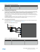
38.8 USB Interface
The USB interface consists of a differential data pair (D+/D-) and a power supply (VBUS, GND).
Refer to the “Electrical Characteristics” on page 935 for operating voltages which will allow USB operation.
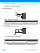
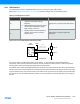
Figure 38-13.Low Cost USB Interface Example Schematic
It is recommended to increase ESD protection on the USB D+, D-, and VBUS lines using dedicated transient
suppressors. These protections should be located as close as possible to the USB connector to reduce the potential
discharge path and reduce discharge propagation within the entire system.
The USB FS cable includes a dedicated shield wire that should be connected to the board with caution. Special attention
should be paid to the connection between the board ground plane and the shield from the USB connector and the cable.
Tying the shield directly to ground would create a direct path from the ground plane to the shield, turning the USB cable
into an antenna. To limit the USB cable antenna effect, it is recommended to connect the shield and ground through an
RC filter.
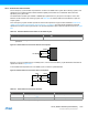
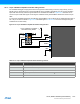
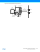
Table 38-12. USB Interface Checklist
Signal Name Recommended Pin Connection Description
D+
z The impedance of the pair should be
matched on the PCB to minimize
reflections.
z USB differential tracks should be routed
with the same characteristics (length,
width, number of vias, etc.)
z Signals should be routed as parallel as
possible, with a minimum number of
angles and vias
USB full speed / low speed positive data upstream
pin
D-
USB full speed / low speed negative data
upstream pin
VBUS
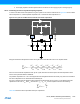
USB
Connector
VBUS
D+
D-
GND
Shield
GND (Board)
USB_D+
USB_D-
USB
Differential
Data Line Pair