
Data Sheet

482
Atmel | SMART SAM D21 [DATASHEET]
Atmel-42181G–SAM-D21_Datasheet–09/2015
26.6.2.4 Data Register
The SPI Transmit Data register (TxDATA) and SPI Receive Data register (RxDATA) share the same I/O address,
referred to as the SPI Data register (DATA). Writing the DATA register will update the Transmit Data register. Reading
the DATA register will return the contents of the Receive Data register.
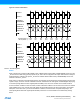
26.6.2.5 SPI Transfer Modes
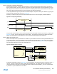
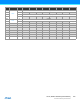
There are four combinations of SCK phase and polarity with respect to the serial data. The SPI data transfer modes are
shown in Table 26-2 and Figure 26-3. SCK phase is selected by the Clock Phase bit in the Control A register
(CTRLA.CPHA). SCK polarity is selected by the Clock Polarity bit in the Control A register (CTRLA.CPOL). Data bits are
shifted out and latched in on opposite edges of the SCK signal, ensuring sufficient time for the data signals to stabilize.
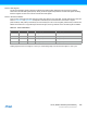
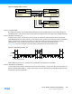
Table 26-2. SPI Transfer Modes
Leading edge is the first clock edge in a clock cycle, while trailing edge is the second clock edge in a clock cycle.
Mode CPOL CPHA Leading Edge Trailing Edge
0 0 0 Rising, sample Falling, setup
1 0 1 Rising, setup Falling, sample
2 1 0 Falling, sample Rising, setup
3 1 1 Falling, setup Rising, sample