
Data Sheet


51
Atmel | SMART SAM D21 [DATASHEET]
Atmel-42181G–SAM-D21_Datasheet–09/2015
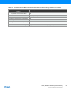
12.4 Signal Description
Refer to “I/O Multiplexing and Considerations” on page 21 for details on the pin mapping for this peripheral.
12.5 Product Dependencies
In order to use this peripheral, other parts of the system must be configured correctly, as described below.
12.5.1 I/O Lines
The SWCLK pin is by default assigned to the DSU module to allow debugger probe detection and the condition to stretch
the CPU reset phase. For more information, refer to “Debugger Probe Detection” on page 52. The Hot-Plugging feature
depends on the PORT configuration. If the SWCLK pin function is changed in the PORT or if the PORT_MUX is disabled,
the Hot-Plugging feature is disabled until a power-reset or an external reset.
12.5.2 Power Management
The DSU will continue to operate in any sleep mode where the selected source clock is running.
Refer to “PM – Power Manager” on page 117 for details on the different sleep modes.
12.5.3 Clocks
The DSU bus clocks (CLK_DSU_APB and CLK_DSU_AHB) can be enabled and disabled in the Power Manager. For
more information on the CLK_DSU_APB and CLK_DSU_AHB clock masks, refer to “PM – Power Manager” on page
117.
12.5.4 DMA
Not applicable.
12.5.5 Interrupts
Not applicable.
12.5.6 Events
Not applicable.
12.5.7 Register Access Protection
All registers with write access are optionally write-protected by the Peripheral Access Controller (PAC), except the
following registers:
z Debug Communication Channel 0 register (DCC0)
z Debug Communication Channel 1 register (DCC1)
Write-protection is denoted by the Write-Protection property in the register description.
Write-protection does not apply for accesses through an external debugger. Refer to “PAC – Peripheral Access
Controller” on page 41 for details.
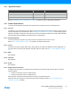
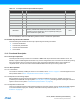
Signal Name Type Description
RESET Digital Input External reset
SWCLK Digital Input SW clock
SWDIO Digital I/O SW bidirectional data pin