
Data Sheet


727
Atmel | SMART SAM D21 [DATASHEET]
Atmel-42181G–SAM-D21_Datasheet–09/2015
1: Compare output is set to DIR when TCC counter matches CCx value.
z Bits 15:12 – Reserved
These bits are unused and reserved for future use. For compatibility with future devices, always write these bits to
zero when this register is written. These bits will always return zero when read.
z Bits 11:8 – CICCENx [x=3..0]: Circular Channel x Enable
Setting these bits enable the compare circular buffer option on channel. When the bit is set, CCx register value is
copied-back into the CCx register on UPDATE condition.
z Bit 7 – CIPEREN: Circular period Enable
Setting these bits enable the period circular buffer option. When the bit field is set, the PER register value is cop-
ied-back into the PERB register on UPDATE condition.
z Bit 6 – Reserved
This bit is unused and reserved for future use. For compatibility with future devices, always write this bit to zero
when this register is written. This bit will always return zero when read.
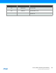
z Bits 5:4 – RAMP[1:0]: Ramp Mode
These bits select Ramp operation (RAMP), as shown in the table below. These bits are not synchronized.
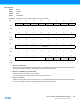
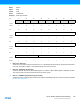
Table 30-26. Ramp Mode
z Bit 3 – Reserved
This bit is unused and reserved for future use. For compatibility with future devices, always write this bit to zero
when this register is written. This bit will always return zero when read.
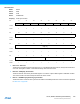
z Bits 2:0 – WAVEGEN[2:0]: Waveform Generation
These bits select the waveform generation operation, as shown in the table below. The settings impact the top
value and select the frequency/PWM mode. These bits are not synchronized.
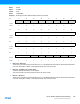
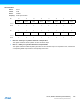
Table 30-27. Waveform Generation
RAMP[1:0] Name Description
0x0 RAMP1 RAMP1 operation
0x1 RAMP2A Alternative RAMP2 operation
0x2 RAMP2 RAMP2 operation
0x3 Reserved
WAVEGEN[2:0] Name Description
0x0 NFRQ Normal frequency
0x1 MFRQ Match frequency
0x2 NPWM Normal PWM
0x3 Reserved
0x4 DSCRITICAL Dual-slope critical