
Data Sheet


846
Atmel | SMART SAM D21 [DATASHEET]
Atmel-42181G–SAM-D21_Datasheet–09/2015
32.5 Product Dependencies
In order to use this peripheral, other parts of the system must be configured correctly, as described below.
32.5.1 I/O Lines
Using the ADC's I/O lines requires the I/O pins to be configured using the port configuration (PORT).
Refer to “PORT” on page 379 for details.
32.5.2 Power Management
The ADC will continue to operate in any sleep mode where the selected source clock is running. The ADC’s interrupts
can be used to wake up the device from sleep modes. The events can trigger other operations in the system without
exiting the sleep modes. Refer to “PM – Power Manager” on page 117 for details on the different sleep modes.
32.5.3 Clocks
The ADC bus clock (CLK_ADC_APB) can be enabled and disabled in the Power Manager, and the default state of
CLK_ADC_APB can be found in the Table 15-1.
A generic clock (GCLK_ADC) is required to clock the ADC. This clock must be configured and enabled in the Generic
Clock Controller (GCLK) before using the ADC. Refer “GCLK – Generic Clock Controller” on page 95 for details.
This generic clock is asynchronous to the bus clock (CLK_ADC_APB). Due to this asynchronicity, writes to certain
registers will require synchronization between the clock domains. Refer to “Synchronization” on page 855 for further
details.
32.5.4 DMA
The DMA request lines are connected to the DMA controller (DMAC). Using the ADC DMA requests, requires the DMA
controller to be configured first. Refer ro “DMAC – Direct Memory Access Controller” on page 272 for details.
32.5.5 Interrupts
The interrupt request line is connected to the interrupt controller. Using ADC interrupts requires the interrupt controller to
be configured first. Refer to “Nested Vector Interrupt Controller” on page 34 for details.
32.5.6 Events
Events are connected to the Event System. Refer to “EVSYS – Event System” on page 406 for details.
32.5.7 Debug Operation
When the CPU is halted in debug mode, the ADC will halt normal operation. The ADC can be forced to continue
operation during debugging. Refer to the Debug Control register (DBGCTRL) for details.
32.5.8 Register Access Protection
All registers with write-access are optionally write-protected by the Peripheral Access Controller (PAC), except the
following register:
z Interrupt Flag Status and Clear register (INTFLAG)
Write-protection is denoted by the Write-Protection property in the register description.
When the CPU is halted in debug mode or the CPU reset is extended, all write-protection is automatically disabled.
Write-protection does not apply for accesses through an external debugger. Refer to “PAC – Peripheral Access
Controller” on page 41 for details.
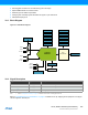
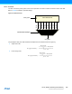
32.5.9 Analog Connections
I/O-pins AIN0 to AIN19 as well as the VREFA/VREFB reference voltage pin are analog inputs to the ADC.