
Data Sheet

968
Atmel | SMART SAM D21 [DATASHEET]
Atmel-42181G–SAM-D21_Datasheet–09/2015
36.10 NVM Characteristics
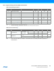
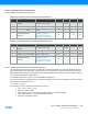
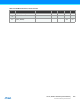
Table 36-39. Maximum Operating Frequency
Note that on this flash technology, a max number of 8 consecutive write is allowed per row. Once this number is reached,
a row erase is mandatory.
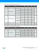
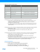
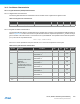
Table 36-40. Flash Endurance and Data Retention
Note: 1. An endurance cycle is a write and an erase operation.
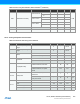
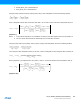
Table 36-41. EEPROM Emulation
(1)
Endurance and Data Retention
Notes: 1. The EEPROM emulation is a software emulation described in the App note AT03265.
2. An endurance cycle is a write and an erase operation.
V
DD
range NVM Wait States Maximum Operating Frequency Units
1.62V to 2.7V
0 14
MHz
1 28
2 42
3 48
2.7V to 3.63V
0 24
1 48
Symbol Parameter Conditions Min. Typ. Max. Units
Ret
NVM25k
Retention after up to 25k Average ambient 55°C 10 50 - Years
Ret
NVM2.5k
Retention after up to 2.5k Average ambient 55°C 20 100 - Years
Ret
NVM100
Retention after up to 100 Average ambient 55°C 25 >100 - Years
Cyc
NVM
Cycling Endurance
(1)
-40°C < Ta < 85°C 25k 150k - Cycles
Symbol Parameter Conditions Min. Typ. Max. Units
Ret
EEPROM100k
Retention after up to 100k Average ambient 55°C 10 50 - Years
Ret
EEPROM10k
Retention after up to 10k Average ambient 55°C 20 100 - Year s
Cyc
EEPROM
Cycling Endurance
(2)
-40°C < Ta < 85°C 100k 600k - Cycles
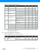
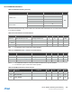
Table 36-42. NVM Characteristics, Device Variant A
Symbol Parameter Conditions Min. Typ. Max. Units
t
FPP
Page programming time - - - 2.5 ms
t
FRE
Row erase time
I
- - - 6 ms
t
FCE
DSU chip erase time
(CHIP_ERASE)
- - - 240 ms