
Data Sheet

Electrical characteristics STM32F030x4/6/8/C
48/96 DocID024849 Rev 2
3. For STM32F030x4/6/8 devices.
4. For STM32F030xC devices only.
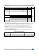
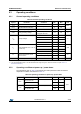
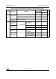
Table 26. Typical and maximum current consumption from the V
DDA
supply
(1)
Symbol Parameter Conditions
(2)
f
HCLK
V
DDA
=
3.6 V
Unit
Typ
Max @ T
A
(3)
85 °C
I
DDA
Supply current in
Run mode, code
executing from Flash
or RAM
HSE bypass, PLL on
48 MHz
(4)
175
(4)
215
(4)
μA
48 MHz
(5)
160
(5)
192
(5)
HSE bypass, PLL off
8 MHz
(4)
3.9
(4)
4.9
(4)
8 MHz
(5)
3.7
(5)
4.6
(5)
1 MHz
(4)
3.9
(4)
4.1
(4)
1 MHz
(5)
3.3
(5)
4.4
(5)
HSI clock, PLL on
48 MHz
(4)
244
(4)
275
(4)
48 MHz
(5)
235
(5)
275
(5)
HSI clock, PLL off
8 MHz
(4)
85
(4)
105
(4)
8 MHz
(5)
77
(5)
92
(5)
Supply current in
Run or Sleep mode,
code executing from
Flash or RAM
HSE bypass, PLL on 48 MHz
(4)
174
(4)
215
(4)
HSE bypass, PLL off
8 MHz
(4)
3.9
(4)
4.9
(4)
1 MHz
(4)
3.9
(4)
4.9
(4)
HSI clock, PLL on 48 MHz
(4)
244
(4)
299
(4)
HSI clock, PLL off 8 MHz
(4)
85
(4)
105
(4)
1. The gray shading is used to distinguish the values for STM32F030xC devices.
2. Current consumption from the V
DDA
supply is independent of whether the digital peripherals are enabled or disabled, being
in Run or Sleep mode or executing from Flash or RAM. Furthermore, when the PLL is off, I
DDA
is independent from the
frequency.
3. Data based on characterization results, not tested in production.
4. For STM32F030x4/6/8 devices.
5. For STM32F030xC devices.