
Data Sheet


Electrical characteristics STM32F030x4/6/8/C
54/96 DocID024849 Rev 2
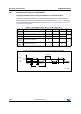
6.3.7 External clock source characteristics
High-speed external user clock generated from an external source
In bypass mode the HSE oscillator is switched off and the input pin is a standard GPIO.
The external clock signal has to respect the I/O characteristics in Section 6.3.14. However,
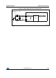
the recommended clock input waveform is shown in Figure 14: High-speed external clock
source AC timing diagram.
Figure 14. High-speed external clock source AC timing diagram
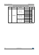
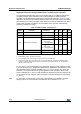
Table 31. High-speed external user clock characteristics
Symbol Parameter
(1)
1. Guaranteed by design, not tested in production.
Min Typ Max Unit
f
HSE_ext
User external clock source frequency 1 8 32 MHz
V
HSEH
OSC_IN input pin high level voltage 0.7 V
DDIOx
-V
DDIOx
V
V
HSEL
OSC_IN input pin low level voltage V
SS
- 0.3 V
DDIOx
t
w(HSEH)
t
w(HSEL)
OSC_IN high or low time 15 - -
ns
t
r(HSE)
t
f(HSE)
OSC_IN rise or fall time - - 20
069
9
+6(+
W
I+6(
7
+6(
W
W
U+6(
9
+6(/
W
Z+6(+
W
Z+6(/