
Data Sheet


DocID024849 Rev 2 71/96
STM32F030x4/6/8/C Electrical characteristics
80
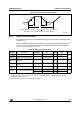
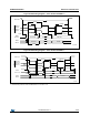
Figure 20. I/O AC characteristics definition
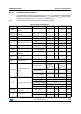
6.3.15 NRST pin characteristics
The NRST pin input driver uses the CMOS technology. It is connected to a permanent pull-
up resistor, R
PU
.
Unless otherwise specified, the parameters given in the table below are derived from tests
performed under the ambient temperature and supply voltage conditions summarized in
Table 21: General operating conditions.
069
7
0D[LPXPIUHTXHQF\LVDFKLHYHGLIWW
ZKHQORDGHGE\&VHHWKHWDEOH,2$&FKDUDFWHULVWLFVGHILQLWLRQ
UI
U,2RXW
W
I,2RXW
W
-
7DQGLIWKHGXW\F\FOHLV
Table 49. NRST pin characteristics
Symbol Parameter Conditions Min Typ Max Unit
V
IL(NRST)
NRST input low level voltage - - - 0.3 V
DD
+0.07
(1)
V
V
IH(NRST)
NRST input high level voltage - 0.445 V
DD
+0.398
(1)
--
V
hys(NRST)
NRST Schmitt trigger voltage
hysteresis
- - 200 - mV
R
PU
Weak pull-up equivalent
resistor
(2)
V
IN
= V
SS
25 40 55 kΩ
V
F(NRST)
NRST input filtered pulse - - 100
(1)
ns
V
NF(NRST)
NRST input not filtered pulse
2.7 < V
DD
< 3.6 300
(3)
--
ns
2.4 < V
DD
< 3.6 500
(3)
--
1. Data based on design simulation only. Not tested in production.
2. The pull-up is designed with a true resistance in series with a switchable PMOS. This PMOS contribution to the series
resistance is minimal (~10% order).
3. Data based on design simulation only. Not tested in production.