
Data Sheet


DocID024849 Rev 2 73/96
STM32F030x4/6/8/C Electrical characteristics
80
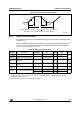
6.3.16 12-bit ADC characteristics
Unless otherwise specified, the parameters given in Table 50 are preliminary values derived
from tests performed under ambient temperature, f
PCLK
frequency and V
DDA
supply voltage
conditions summarized in Table 21: General operating conditions.
Note: It is recommended to perform a calibration after each power-up.
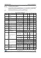
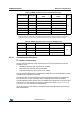
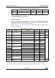
Table 50. ADC characteristics
Symbol Parameter Conditions Min Typ
Max Unit
V
DDA
Analog supply voltage for
ADC ON
- 2.4 - 3.6 V
I
DDA (ADC)
Current consumption of
the ADC
(1)
V
DD
= V
DDA
= 3.3 V - 0.9 - mA
f
ADC
ADC clock frequency - 0.6 - 14 MHz
f
S
(2)
Sampling rate - 0.05 - 1 MHz
f
TRIG
(2)
External trigger frequency
f
ADC
= 14 MHz - - 823 kHz
- - - 17 1/f
ADC
V
AIN
Conversion voltage range - 0 - V
DDA
V
R
AIN
(2)
External input impedance
See Equation 1 and
Table 51 for details
- - 50 kΩ
R
ADC
(2)
Sampling switch
resistance
---1kΩ
C
ADC
(2)
Internal sample and hold
capacitor
---8pF
t
CAL
(2)
Calibration time
f
ADC
= 14 MHz 5.9 μs
- 83 1/f
ADC
W
LATENCY
(2)
ADC_DR register write
latency
ADC clock = HSI14
1.5 ADC
cycles + 2
f
PCLK
cycles
-
1.5 ADC
cycles + 3
f
PCLK
cycles
ADC clock = PCLK/2 - 4.5 -
f
PCLK
cycle
ADC clock = PCLK/4 - 8.5 -
f
PCLK
cycle
t
latr
(2)
Trigger conversion latency
f
ADC
= f
PCLK
/2 = 14 MHz 0.196 μs
f
ADC
= f
PCLK
/2 5.5 1/f
PCLK
f
ADC
= f
PCLK
/4 = 12 MHz 0.219 μs
f
ADC
= f
PCLK
/4 10.5 1/f
PCLK
f
ADC
= f
HSI14
= 14 MHz 0.188 - 0.259 μs
Jitter
ADC
ADC jitter on trigger
conversion
f
ADC
= f
HSI14
-1-1/f
HSI14
t
S
(2)
Sampling time
f
ADC
= 14 MHz 0.107 - 17.1 μs
1.5 - 239.5 1/f
ADC