INSTRUCTION MANUAL Sensoray Model 7405 STDbus Analog Output Card 01/10/2000 Sensoray Co., Inc. 7313 SW Tech Center Dr., Tigard, Oregon 97223 voice: 503.684.8005, fax: 503.684.8164, e-mail: sales@sensoray.com www.sensoray.
Limited Warranty Sensoray Company, Incorporated (Sensoray) warrants the model 7405 hardware to be free from defects in material and workmanship and perform to applicable published Sensoray specifications for two years from the date of shipment to purchaser. Sensoray will, at its option, repair or replace equipment that proves to be defective during the warranty period. This warranty includes parts and labor.
Hardware Configuration The Model 7405 requires the installation of programming shunts to select various options such as I/O port addresses and channel operating modes. This section describes these configuration options. After configuring the option shunts, the Model 7405 may be installed in your STDbus backplane and programmed as explained in the Programming section of this manual. Both board address and channel output types are established by installing programming shunts at various locations on the board.
Programming Model Data Registers The Model 7405 board occupies two contiguous I/O ports in the STDbus I/O space. Both ports may be written to, and the base port has a read function as well. Analog channel data may be written into the A and B registers after ensuring that the status register handshake bits are both reset to logic 0.
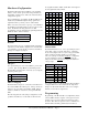
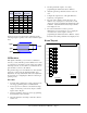
Chan 0 1 2 3 4 5 6 7 5. Set analog channel 0 output to -10 volts by programming the channel data value to 000 hex. Voltage Mode Pin Current Mode Pin 6. Adjust the gain trimpot until the voltmeter reads -10 volts. + - + - 7. 2 6 10 14 18 22 26 30 4 8 12 16 20 24 28 32 1 5 9 13 17 21 25 29 3 7 11 15 19 23 27 31 Configure the output modes of all eight channels as required by your application. 8. For each voltage channel, connect the meter to the channel voltage output pins on connector P1.
Sample Drivers These sample driver functions, written in C/C++, assume that all channels are configured for the voltage output mode. With minor modification, these drivers can be made to work with channels that are set up for current output mode operation.
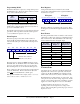
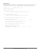
D C B A * P2 A0 A1 A2 A3 A4 A5 A6 A7 A8 A9 A10 A11 A12 A13 A14 A15 D0 D1 D2 D3 D4 D5 D6 D7 VBB1 VBB2 +5V +5V DGND DGND AGND AGND +12V -12V WR RD IORQ MEMRQ IOEXP MEMEX RFSH MSYNC STAT1 STAT0 BUSAK BUSRQ INTAK INTRQ WAITRQ NMIRQ SYSRESET PBRESET CLOCK CNTRL PCO PCI E8 E1 E2 E3 E4 E5 E6 E7 BOARD ADDRESS SELECT JUMPERS 1 53 54 55 56 +5V +12V -12V AB0 AB1 AB2 AB3 AB4 AB5 AB6 AB7 29 27 25 23 21 19 17 15 30 28 26 24 22 20 18 16 31 32 33 34 35 36 37 38 39 40 41 42 43 44 45 46 47 48 49 50 51 52
D C B A DGND D[0..11] 1 GAIN -12V -12V AGND +12V - + R66 GAIN 500-POT D0 D1 D2 D3 D4 D5 D6 D7 D8 D9 D10 D11 12 15 16 14 13 11 10 9 8 7 6 5 4 3 2 10.0K,1% +12V 2 AD7845 DGND WR CS D0 D1 D2 D3 D4 D5 D6 D7 D8 D9 D10 D11 U18 3 5 AGND VOUT VREF VSS VDD RFB RC RB RA U11A MC34082 1 C45 0.1uF 24 23 22 21 -12V VREF Q10 MPS6601 18 1 17 19 20 VREF* -12V +12V VREF Q9 2N4403 VREF* R79 10.0K,1% C46 0.