Preliminary Datasheet SEQUANS Communications 15-55 Boulevard Charles de Gaulle 92700 Colombes, France Phone. +33.1.70.72.16.00 Fax. +33.1.70.72.16.09 www.sequans.com contact@sequans.
Product Summary 1 1.1 General Description The Monarch 2 GM02S is an LTE Cat M1/NB1/NB2 module based on Sequans' second generation Monarch 2 chip platform. GM02S is a total module solution, including a complete, Single-SKU™ RF front end for deployment in any band worldwide, and an integrated EAL5+ Secure Element (SE) enabling the integration of the SIM inside the module with zero compromise on security while lowering cost and reducing complexity.
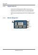
PRODUCT SUMMARY APPLICATIONS 1.3 Applications GM02S is ideal for adding LTE-M and/or NB-IoT LTE connectivity to narrowband, low data rate M2M and IoT devices, including utility meters, industrial sensors, health and fitness bands, asset trackers, and numerous additional devices for smart home, smart city, and wearable applications. GM02S can be used by applications as slim modem controlled by an external MCU via UART. Alternatively, applications may run on GM02S' integrated MCU. 1.
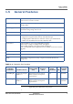
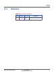
PRODUCT SUMMARY GENERAL FEATURES 1.5 General Features Physical Characteristics LGA module, 100 pads Size: 16.3 mm x 17 mm x 1.85 mm Temperature Range Operation temperature range: -40°C to +85 °C Storage: MSL3 Power Supply Voltage range for RF compliancy: 2.5V to 5.5V Functional voltage range: 2.2V to 5.5V Tx Power +23 dBm for each band Interfaces • Dual (U)SIM Card Interface: support for external, removable or fixed UICC.
Interfaces 2 2.
INTERFACES ANTENNA 2.
INTERFACES POWER 2.3 Power 2.3.1 Power Details Note: Pad 1V8 is the reference voltage for IOs. It can be used to provide power small devices (100 mA maximum usage). This voltage is not available when the modem is in Deep Sleep. When the modem is in standby the voltage drops to 1.62V as per Table 2-2. Table 2-2: Power Pads Pad # Power Group Pad Name Direction Min Operational Value Typical Operational Value Max Operational Value 8 1V8 See note above PVDD_1V8 Out 1.62 V 1.8 V 1.
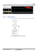
INTERFACES POWER Figure 2-3: Timing Diagram for Reset Sequence 2.3.2 Power States Figure 2-4 represents the electrical states of the module and their transitions.
INTERFACES POWER The various power modes are described in Table 2-4 and illustrated on Figure 2-5.
INTERFACES UART 2.4 UART GM02S, when used as a slim modem, has three UARTs available. While the function of the UARTs can be configured, the default function for each UART is as follows: • UART0: data and control from external MCU via AT commands • UART1: debug and upgrade • UART2: modem console In addition, a fourth UART (UART3) may be used when running applications on GM02S.
INTERFACES UART 31 CTS1 CTS1 State @reset Pad type2 Direction Alternate Function1 Pad Name Primary Function Pad # Power Group Table 2-5: UART Signals (Continued) N/A PVDD_1V8 Out BIDIR Out-1, 2mA N/A PMU_5V In IN HighZ In/Out BIDIR HighZ, 2mA In/Out BIDIR Out-1, 2mA UART1 29 RTS1 RTS1 Wake signal enabled by default.
INTERFACES UART GPIO22 RTS3 PVDD_1V8 In/Out BIDIR State @reset Pad type2 GPIO22/RTS3 Alternate Function1 Pad Name Direction 23 Primary Function Pad # Power Group Table 2-5: UART Signals (Continued) Out-1, 2mA UART3 1. Alternate functions will be available in future versions via SW upgrade. 2.UART pad types’s electrical characteristics are detailed in Table 2-15. High-Speed UARTs Flow Control Signals • CTS0, CTS1, CTS2, CTS3: resp.
INTERFACES USIM INTERFACES 2.5 USIM Interfaces 2.5.1 SIM0 Interface This is the main external SIM interface. It can be used with removable or non-removable SIM cards or with soldered SIM chips. The power supply of the SIM is managed by the modem to ensure lowest power consumption of the SIM.
INTERFACES I2C 2.5.2 SIM1 Interface This interface can be used as a second SIM interface for GM02S, typically used for soldered SIM chips (since it lacks SIM detect and SIM VCC). If design only has one SIM, it is preferred then to use the main SIM interface (see Section SIM0 Interface above).
INTERFACES PCM 2.7 PCM State @reset Pad type2 Direction Power Group Pad Name Alternate Function1 Pad # Primary Function Table 2-9: PCM Pad Details 96 GPIO4/ PCM_CLK GPIO4 PCM_CLK PVDD_1V8 In/Out BIDIR HighZ 98 GPIO3/ PCM_RXD GPIO3 PCM_RXD PVDD_1V8 In/Out BIDIR HighZ 99 GPIO5/ PCM_FS GPIO5 PCM_FS PVDD_1V8 In/Out BIDIR HighZ 100 GPIO6/ PCM_TXD GPIO6 PCM_TXD PVDD_1V8 In/Out BIDIR HighZ 1. Alternate functions will be available in future versions via SW upgrade. 2.
INTERFACES SPI 2.8 SPI Pad type2 State @reset 3 GPIO7/ SPI_SDI GPIO7 SPI_SDI PVDD_1V8 In/Out BIDIR HighZ 4 GPIO8/ SPI_SDO GPIO8 SPI_SDO PVDD_1V8 In/Out BIDIR HighZ 2 GPIO9/ SPI_CLK GPIO9 SPI_CLK PVDD_1V8 In/Out BIDIR HighZ 5 GPIO10/ SPI_CSN1 GPIO10 SPI_CSN1 PVDD_1V8 In/Out BIDIR HighZ 7 GPIO11/ SPI_CSN2 GPIO11 SPI_CSN2 PVDD_1V8 In/Out BIDIR HighZ Pad # Primary Function Direction Power Group Alternate Function1 Table 2-10: SPI Pad Details Pad Name 1.
INTERFACES GPIO 2.9 GPIO There is a total of 33 GPIOs available on GM02S: 28 named GPIO1 to GPIO28 and 5 named GPIO31 to GPIO35. The GPIOs listed in Table 2-11 are not enabled by default. Changing their state can be done by software. Table 2-11: GPIOs Disabled by Default GPIO Range Enable State by Default GPIO3 to GPIO11 Disabled GPIO17 to GPIO28 Disabled GPIO31 to GPIO32 Disabled The GPIOs are documented throughout this datasheet based on their shared or assigned function.
INTERFACES OTHER SIGNALS 2.
INTERFACES OTHER SIGNALS 9 TX_IND GPIO33 PVDD_1V8 In/Out State @reset Pad Type2 Direction Name GPIO33/ TX_IND Alternate Function1 Primary Function Pad # Power Group Table 2-13: Other Signals (No Interface) (Continued) BIDIR HighZ, 2mA Primary Function: Transmission indicator (TX_IND, OUT). Active high.
INTERFACES OTHER SIGNALS 47 WAKE1 N/A PMU_5V In State @reset Pad Type2 Direction Name WAKE1 Alternate Function1 Primary Function Pad # Power Group Table 2-13: Other Signals (No Interface) (Continued) IN HighZ IN HighZ IN HighZ IN HighZ Wake #1 input line (WAKE1, IN), diabled by default. 49 WAKE2 WAKE2 N/A PMU_5V In Wake #2 input line (WAKE2, IN), diabled by default. 55 WAKE3 WAKE3 N/A PMU_5V In Wake #3 input line (WAKE3, IN), diabled by default.
INTERFACES JTAG 2.11 JTAG State @reset Pad type1 Direction Pad Name Power Group Pad # Primary Function Table 2-14: JTAG Pad Details 69 JTAG_TCK JTAG_TCK PVDD_1V8 In IN In Pull-down Schmitt-trigger 67 JTAG_TDI JTAG_TDI PVDD_1V8 In IN In, Pull-up 68 JTAG_TDO JTAG_TDO PVDD_1V8 Out BIDIR Out, 0 66 JTAG_TMS JTAG_TMS PVDD_1V8 In IN In, Pull-up 70 JTAG_TRSTN JTAG_TRSTN PVDD_1V8 In IN In, Pull-down 1.
INTERFACES DIGITAL IO CHARACTERISTICS 2.12 Digital IO Characteristics The voltage and current characteristics of the various IO pads of the GM02S versus IO bank supply voltage are illustrated in the tables below. Caution: The PCB designer must ensure that the voltage on these pads never exceeds Vih of the power group to which they belong. See Table 2-15 for digital IO characteristics of the different IO pads.
INTERFACES DIGITAL IO CHARACTERISTICS Table 2-15: DC Characteristics for Digital IOs, Voltage 1.
Mechanical Characteristics 3 3.1 Package Description The package size with tolerance is: (16.3 ± 0.1) mm x (17.0 ± 0.1) mm x (1.
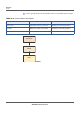
MECHANICAL CHARACTERISTICS PACKAGE DESCRIPTION Figure 3-2: GM02S PCB View Note: Gxx pads should be grounded to a large ground plane on customer's PCB layer 1. It is also recommended to have the Gxx pads area in the PCB through ground vias to improve thermal dissipation efficiency. Table 3-1: GM02S Dimensions (mm) Dimension 24 Value (mm) L 16.3 ± 0.1 W 17.0 ± 0.1 T 1.85 max T0 0.5 max L1 0.5 ± 0.1 W1 0.7 ± 0.1 L2 0.8 ± 0.1 W2 0.8 ± 0.1 a1 2.25 ± 0.1 a2 3.05 ± 0.
MECHANICAL CHARACTERISTICS PACKAGE DESCRIPTION Table 3-1: GM02S Dimensions (mm) (Continued) Dimension GM02S DATASHEET (PRELIMINARY) Value (mm) a3 1.45 ± 0.1 a4 2.45 ± 0.1 a5 6.5 ± 0.1 b1 2.0 ± 0.1 b2 3.0 ± 0.1 b3 3.1 ± 0.1 b4 5.5 ± 0.1 b5 5.95 ± 0.1 P1 0.3 ± 0.1 P2 0.3 ± 0.1 P3 0.4 ± 0.1 P4 0.4 ± 0.
MECHANICAL CHARACTERISTICS PACKAGE DESCRIPTION Figure 3-3: GM02S Laser Marking (Preliminary) Notes on Figure 3-3: 1. FCC ID: 2AAGMGM02S 2. IC: 12732A-GM02S 3. IMEI:XXXXXXXXXXXXXXX 4. ICCID:XXXXXXXXXXXXXXX (for future support) 5. S/N:G2HYYMMDDNNNNSSS (16 digits) • G2H: reserved (3 digits) • YYMMDD: Manufacturing Date (YY:Year;MM:Month,DD:Day) • NNNN: Panel counter (from 0001~9999) • SSS: Piece location on panel (from 001~036) 6. 2D marked "a" refer to IMEI Barcode 7.
MECHANICAL CHARACTERISTICS ENVIRONMENTAL CONDITIONS 3.
MECHANICAL CHARACTERISTICS PACKING 3.3 Packing The GM02S is delivered in Tape-and-Reel. Details are provided in the figures below.
MECHANICAL CHARACTERISTICS STORAGE AND MOUNTING 3.4 Storage and Mounting The GM02S module is Moisture Level 3 rated as per JEDEC industrial standard: http://www.ipc.org/TOC/J-STD-033D-TOC.
4 GM02S DATASHEET (PRELIMINARY) Regulatory Approval • RED regulatory approval details will be provided in a future revision of this document. • TELEC regulatory approval details will be provided in a future revision of this document.
REGULATORY APPROVAL FCC REGULATORY APPROVAL 4.1 FCC Regulatory Approval FCC-ID: 2AAGMGM02S (single modular approval) This above identified LTE radio module is not intended to be provided to end-users but is for installation by OEM integrators only.
REGULATORY APPROVAL FCC REGULATORY APPROVAL End-product Labelling • FCC-ID The module's FCC-ID must either be visible from the exterior of the host product (e.g. per window) or per electronic display, or shall be displayed on an additional exterior label per the following or similar string: contains FCC-ID: 2AAGMGM02S • Digital Device - Unwanted Emissions Notice If the end-product falls under part 15 of the FCC rules (it shall display the following user notice on its exterior acc. to part 15.
REGULATORY APPROVAL FCC REGULATORY APPROVAL • Digital Device - Unwanted Emissions Notice If the end-product is or contains a digital device (unintentional radio portions) and is not exempted by its use case (like vehicular use) the following part 15.105 (b) user notice shall be provided at prominent location of the product literature: This equipment has been tested and found to comply with the limits for a Class B digital device, pursuant to part 15 of the FCC rules.
REGULATORY APPROVAL INDUSTRY CANADA STATEMENT 4.2 Industry Canada Statement This device complies with ISED’s licence exempt RSSs. Operation is subject to the following two conditions: (1) This device may not cause harmful interference, and (2) this device must accept any interference received, including interference that may cause undesired operation. Le présent appareil est conforme aux CNR d’ ISED applicables aux appareils radio exempts de licence.
REGULATORY APPROVAL INDUSTRY CANADA STATEMENT NOTE IMPORTANTE: Dans le cas où ces conditions ne peuvent être satisfaites (par exemple pour certaines configurations d'ordinateur portable ou de certaines co localisation avec un autre émetteur), l'autorisation du Canada n'est plus considéré comme valide et l'ID IC ne peut pas être utilisé sur le produit final.
A Acronyms Acronym Definition ADC Analog to Digital Converter CPU Central Processing Unit DL Downlink ESD Electro-static discharge ETSI European Telecommunications Standard Institute GND Ground GPIO General Purpose Input Output I/O Input/Output I2C Inter-Integrated Circuit interface IMEI International Mobile Equipment Identity IP Internet Protocol JTAG Joint Test Action Group LGA Large Grid Array LTE Long Term Evolution, or 4G. Standard is developed by the 3GPP www.3gpp.org.
Acronym Definition RED European Radio Equipment Directive RF Radio Frequency RoHS Restriction of Hazardous Substances Rx Reception S/N or SN: Serial Number SIM Subscriber Identification Module SMS Short Message Service SPI Serial Peripheral Interface Tx Transmission UART Universal Asynchronous Receiver Transmitter UE User Equipment UL Uplink USB Universal Serial Bus GM02S DATASHEET (PRELIMINARY) PROPRIETARY SEQUANS Communications 37
About this Datasheet Purpose and Scope The GM02S is a complete LTE Cat M1/NB1/NB2 module including base-band, RF and memory, for the design of narrowband low data rate M2M and IoT devices for wide deployment. This document provides technical information about GM02S LGA module. GM02S is based on Sequans' Monarch 2 platform. Who Should Read this Document This document is intended for engineers who are developing User Equipment (UE) for LTE systems.
Changes in this Document The following changes were done since the previous edition of this document: GM02S DATASHEET (PRELIMINARY) • Updated part numbers details in .Table 1-1 on page 3 • Added timing diagrams in Section 2.3 Power on page 6. • Added Section 2.3.2 Power States on page 7. • Added default Enable status for GPIOs in Section 2.9 GPIO on page 16 • Added RING0 polarity information in Table 2-13. • Restrict usage for Pad #53 to Reserved in Table 2-13 and signals list.
Table of Contents Chapter 1 Product Summary . . . . . . . . . . . . . . . . . . . . . . . . . . . . . . . . 1 1.1 General Description . . . . . . . . . . . . . . . . . . . . . . . . . . . . . . . . . . . . . . . . . . . . . . . . . . . . . . 1 1.2 Frequency Bands. . . . . . . . . . . . . . . . . . . . . . . . . . . . . . . . . . . . . . . . . . . . . . . . . . . . . . . . . 1 1.3 Applications . . . . . . . . . . . . . . . . . . . . . . . . . . . . . . . . . . . . . . . . . . . . . . . . . . . . . . . .
Table of Contents 4.2 Industry Canada Statement . . . . . . . . . . . . . . . . . . . . . . . . . . . . . . . . . . . . . . . . . . . . . . . . 34 Appendix A Acronyms . . . . . . . . . . . . . . . . . . . . . . . . . . . . . . . . . . . . 36 About this Datasheet . . . . . . . . . . . . . . . . . . . . . . . . . . . . . 38 Purpose and Scope . . . . . . . . . . . . . . . . . . . . . . . . . . . . . . . . . . . . . . . . . . . . . . . . . . . . . . . . . . . . . . . . . 38 Who Should Read this Document .