Shanghai MacroGiga Electronics Ltd. Co. MG223, BLE Transmitter Data Sheet Revision History: Rev. No. History Issue Date 0.1 Draft Nov 15, 2020 0.2 Update Electrical Characteristics Dec 25, 2020 1.0 Update package info July 23, 2021 Remark Release Important Notice: MACROGIGA reserves the right to make changes to its products or to discontinue any integrated circuit product or service without notice.
Shanghai MacroGiga Electronics Ltd. Co. Table of Contents 1. Overview................................................................................................................................................3 1.1 Features........................................................................................................................................... 3 1.2 Typical Application.......................................................................................................................
Shanghai MacroGiga Electronics Ltd. Co. 1. Overview MG223 is a single mode BLE RF transmitter with software configurable registers, embedded packet handling engine, and designed for ultra low power Bluetooth Smart Devices. The chip is configured and operated via the 3-wire SPI(Serial Peripheral Interface) or I2C interface. Internal voltage regulators ensure a high Power Supply Rejection Ratio (PSRR) and a wide power supply range(2.0~3.6V). MG223 is pin-to-pin compatible with MG123. 1.
Shanghai MacroGiga Electronics Ltd. Co. 3-wire hardware SPI, Max 10Mbps I2C interface Power Management Integrated voltage regulator 2.0 to 3.6V supply range Idle modes with fast start-up times for advanced power management 4uA in sleep mode 0.2uA in standby mode Low cost BOM Provides a single-ended RF port pin No matching components needed Built-in 32KHz oscillator Support low cost crystal(16MHz) 1.2 Typical Application Beacon transmitter Remote Controller Revision: 1.
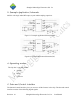
Shanghai MacroGiga Electronics Ltd. Co. 1.3 Block Diagram Figure1.1 Block Diagram 2. Pin Description Pin No. Symbol I/O Function Description 1 SCK DI SPI Clock / I2C_SCL 2 DVDD AO Digital VDD 1.2v Output 3 MOSI DI SPI Slave Data Input / I2C_SDA 4 XTALO AO Crystal Pin 5 XTALI AI Crystal Pin 6 ANT RF Antenna interface 7 GND Power Ground(0V) 8 VBAT Power Power Supply 9 nRST AI Chip reset pin 10 CSN DI SPI Chip Select Table2.1 Revision: 1.
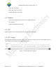
Shanghai MacroGiga Electronics Ltd. Co. 3. Example Application Schematic MG223 with single ended RF output, crystal and decoupling capacitors. Figure 3.1 Example Application Schematic(SPI) Figure 3.2 Example Application Schematic(I2C) 4. Operating modes The chip has 3 operating modes: Standby Sleep TX active 5. Data and Control Interface The data and control interface gives you access to all the features in the chip.
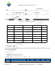
Shanghai MacroGiga Electronics Ltd. Co. • CSN (SPI_CS signal) • SCK (SPI_SCK or I2C_SCL) • MOSI (SPI data or I2C_SDA) 5.1 Features • 3-wire SPI serial interface, as slave, up to 10Mbps data rate • I2C interface • Easily configurable register map 5.2 I2C When working in I2C, CSN pin should leave floating (Not Connected)。 5.3 SPI Timing SPI operation and timing is given in Figure 5.3.1. The device must be in one of the standby modes or sleep mode before writing to the configuration registers. Figure 5.3.
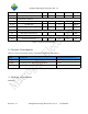
Shanghai MacroGiga Electronics Ltd. Co. Figure 5.3.2 SPI timing diagram Symbol Parameters Min. Max Unit Tcc CSN to SCK setup 2 - ns Tch SCK high time 40 - ns Tcl SCK low time 40 - ns Tcwh CSN inactive time 50 - ns Tcch SCK to CSN hold 2 - ns Tdc Data to SCK setup 2 - ns Tdh SCK to Data hold 2 - ns 6. Register Map You can configure and control the radio chip by accessing the register map through SPI or I2C by using read and write commands. 7.
Shanghai MacroGiga Electronics Ltd. Co. VDD Supply voltage 2.0 3.0 3.6 V TEMP Operating Temperature -40 +27 +85 ℃ 2480 MHz General RF condition fOP Operating frequency 2402 RGFSK Air data rate 1, 2 Mbps Fchannel Non-overlapping channel spacing 2 MHz Transmitter Operation condition PRF Maximum output power +3.5 dBm 10.3 ms Power on Reset TPOR Power on reset time 1.5 5.3 Table 7.1 Electrical Specification 8. Current Consumption Table 8.
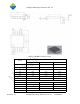
Shanghai MacroGiga Electronics Ltd. Co. Table 9.1 MSOP10 Package outline Symbol Dimensions in Millimeters Min. NOM Max. A 0.82 - 1.10 A1 0.02 - 0.15 A2 0.75 - 0.95 A3 0.30 0.35 0.40 D 2.90 3.00 3.10 E 4.70 4.90 5.10 E1 2.90 3.00 3.10 e b 0.18 - 0.28 c 0.09 - 0.23 θ 0 - 6o L 0.40 - 0.80 L1 Revision: 1.0 0.50BSC o 0.95REF Shanghai MacroGiga Electronics Ltd. Co.
Shanghai MacroGiga Electronics Ltd. Co. 10. Reflow Profile Revision: 1.0 Shanghai MacroGiga Electronics Ltd. Co.
Federal Communications Commission (FCC) Statement. This device complies with part 15 of the FCC Rules. Operation is subject to the following twoconditions: (1) This device may not cause harmful interference, and (2) this device must accept any interference received, including interference that may cause undesired operation. Note: This equipment has been tested and found to comply with the limits for a Class B digital device, pursuant to part 15 of the FCC Rules.
Integration instructions for host product manufacturers according to KDB 996369 D03 OEM Manual v01 2.2 List of applicable FCC rules FCC Part 15.247. 2.3 Specific operational use conditions This module is stand-alone modular. If the end product will involve the Multiple simultaneously transmitting condition or different operational conditions for a stand-alone modular transmitter in a host, host manufacturer have to consult with module manufacturer for the installation method in end system. 2.