L506 Hardware Design L506 Hardware Design LTE Module Series Version: V1.
L506 Hardware Design Notice Some features of the product and its accessories described herein rely on the software installed, capacities and settings of local network, and therefore may not be activated or may be limited by local network operators or network service providers. Thus, the descriptions herein may not exactly match the product or its accessories which you purchase.
L506 Hardware Design FCC Caution: (1)Exposure to Radio Frequency Radiation. This equipment must be installed and operated in accordance with provided instructions and the antenna(s) used for this transmitter must be installed to provide a separation distance of at least 20 cm from all persons and must not be collocated or operating in conjunction with any other antenna or transmitter.
L506 Hardware Design Version History Date Version Description of change 2020-06-01 V1.
L506 Hardware Design Contents 1 ABOUT THIS DOCUMENT ...................................... 8 1.1 Applicable scope ....................................................................................................................................... 8 1.2 Writing purpose ....................................................................................................................................... 8 1.3 Support and reference documents list ............................................................
L506 Hardware Design 3.5 USIM interface ....................................................................................................................................... 31 3.5.1 Pin definition ......................................................... 31 3.5.2 Design Guide ........................................................... 32 3.5.3 USIM interface reference circuit ....................................... 32 3.6 PCM interface ....................................................................
L506 Hardware Design 4.2.3 current consumption .................................................... 53 4.3 Working and storage temperature ....................................................................................................... 54 4.4 ESD performance .................................................................................................................................. 54 5 DESIGN GUIDELINE ........................................ 55 5.1 General design rules and requirements ......
L506 Hardware Design 1 About this document 1.1 Applicable scope This document describes theL506series 4G LTE LCC Module (hereinafter referred to as L506), the basic specifications, product electrical characteristics, design guidance and hardware interface development guidance. Users need to follow this documentation requirements and guidance for design. This document applies only to L506 products in the application development. 1.
L506 Hardware Design Table 1-1 support document list No. Documents 1 《L506AT Command User Guide》 2 《L506_SPEC.docx》 3 《L506EVBUserManual》 4 《L506Schematic checklist》 5 《L506Layout checklist》 6 《L506_Reference Design_V3.pdf》 7 《L506_V3_DECAL.sch》 8 《L506_V3_DECAL.PCB》 1.
L506 Hardware Design HSDPA High Speed Downlink Packet Access HSUPA High Speed Uplink Packet Access AGPS Assisted Global Positioning System BER Bit Error Rate DL Downlink COEX WLAM/LTE-ISM coexistence SMPS Switched-mode power supplies LTE Long Term Evolution FDD Frequency Division Duplexing TDD Time Division Duplexing DPCH Dedicated Physical Channel DPCH_Ec Average energy per PN chip for DPCH.
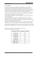
L506 Hardware Design LTE 能力 CAT4 CAT1 Data transmission specifications LTE-FDD CAT4 - Uplink up to 50 Mbps, - Downlink up to 150 Mbps LTE-FDD CAT1 - Uplink up to 5 Mbps - Downlink up to 10 Mbps WCDMA-HSPA+ - Uplink up to 5.76 Mbps - Downlink up to 42 Mbps Interface SUB2.0 UART USIM (2.85V/1.8V) GPIO ADC SDIO PCM SPI I2C NETLIGHT POWER KEY RESET Dimensions(L×W×H):30mm×30mm×2.
L506 Hardware Design 2.1 Package Dimensions The product module is 87-PIN LCC package module, in addition to signal pin, also contains many special heat welding disc to improve joint performance, mechanical strength and heat dissipation performance, the heat release welding disc 12 and uniform distribution in the bottom of the PCB. Package size is 30 x 30 mm, the height is 2.8 mm.
L506 Hardware Design (c)Bottom Dimensions (Unit mm) Note: antenna feed point in actual use of the customers don't need (PCB assembly, the stencil file).
L506 Hardware Design (d)Bottom Detail B (Unit mm) Copyright© Shanghai Mobiletek Communication Ltd 14
L506 Hardware Design (e)Bottom Detail C(Unit mm) Copyright© Shanghai Mobiletek Communication Ltd 15
L506 Hardware Design (e)Side view Dimensions(Unit mm) Figure 2-2Module Dimensions 2.2 Product Function Outline 2.2.1 Hardware Diagram This product mainly includes the following signal group:USB Interface signal、USIM card Interface signal、I2C Interface signal、UART Interface signal、PCM Interface signal、UART Interface signal、 WIFI Interface signal(WIFI Version)、SPI interface、Module startup、Module control signal、Power supply and ground.
L506 Hardware Design MAIN ANT FLASH DDR SDIO/IO PCM/I2S UART/SPI GNSS IQ RF Transceiver Baseband RF IQ SD CARD CLK DATA RF SWITCH SIM CARD VBAT I/O STATUS RF WCDMA/FDD-LTE PA VDD_RF PMIC VBAT LDO 19.2 MHZXO VBAT VBAT Power on/off Reset Figure 2-3 L506 System Functional Architecture 2.2.
L506 Hardware Design UMTS850 24dBm +1/-3dB <-50dBm UMTS2100 24dBm +1/-3dB <-50dBm FDD_LTE B1 23dBm +/-2.7dB <-40dBm FDD_LTE B3 23dBm +/-2.7dB <-40dBm FDD_LTE B4 23dBm +/-2.7dB <-40dBm FDD_LTE B5 23dBm +/-2.7dB <-40dBm FDD_LTE B28A 23dBm +/-2.7dB <-40dBm FDD_LTE B28B 23dBm +/-2.
L506 Hardware Design 3 Interface Description 3.1 PIN Definition 3.1.1 Pin I/O parameter definition The I/O parameter definition of the product is shown in table 3-1.
GND VBAT VBAT GND BOOT_CFG 1 63 62 61 87 GND 65 64 CTS RTS 66 68 67 RI RXD 69# TXD DCD 70 DTR 71 PCM_OUT PCM_IN 74 73 PCM_SYNC 75 72# GND PCM_CLK 76 GND 78 77 GND RESERVED 79 COEX3 80 86 L506 Hardware Design 85 GND 2 PWRKEY 3 SPI_MISO 7 SPI_MOSI 8 SPI_CS 9 GND 10 USB_DP 13 GND 14 USB_ID 16 USIM_DATA 17 18 USIM_CLK 19 USIM_VDD 20 39 VBAT 83 38 VBAT 40 37 GND GND 36* COEX1 35* SDC1_CLK 31* SDC1_DATA3 34* 30* WLAN_EN VREG_L2_1V8 2
L506 Hardware Design 7 SPI_MISO 8 SPI_MOSI 9 SPI_CS 10 GND 11 USB_VBUS 12 USB_DN 13 USB_DP 14 GND 15 VDD_1V8 16 USB_ID 17 USIM_DATA 18 USIM_RST 19 USIM_CLK 20 USIM_VDD 21 SD_CMD 22 SD_DATA0 23 SD_DATA1 24 SD_DATA2 25 SD_DATA3 26 SD_CLK 27* SDC1_DATA2 28# GPIO_3 29* SDC1_DATA1 30* WLAN_EN 31* SDC1_DATA3 32* SDC1_CMD 33* SDC1_DATA0 34* VREG_L2_1V8 35* WLAN_32K_SLEEP_CLK 36* SDC1_CLK 37 GND 38 VBAT 39 VBAT 40 GND 41 GND 42* WIFI3V3_EN 43
L506 Hardware Design 71 TXD 72# DTR 73 PCM_OUT 74 PCM_IN 75 PCM_SYNC 76 PCM_CLK 77 GND 78 GND 79 RESERVED 80 GND 81 GND 82 MAIN_ANT 83 COEX1 84 COEX2# 85 BOOT_CFG0 86 COEX3 87 BOOT_CFG1 Table 3-3 Pin Function Description Power interface Pin Name Pin No. I/O Description Content Power supply voltage, VBAT 38,39,62,63 PI VBAT=3.4V~4.2V. The power supply for system Maximum load current must above 2A. Module LDO output power ,1.
L506 Hardware Design flight mode; L: normal mode Module status(GPIO) Pin Name Pin No. I/O NETLIGHT 51 DO Description Identify the 40 DO system network status. Module STATUS Content status identify: High level power on, low level power off. WIFI/BT interface(WIFI Version) Pin name Pin No.
L506 Hardware Design keep it open Default: GPIO GPIO_3/BT_EN 28 I/O Optional: BT_EN for ext bt pin module If not use keep it open enable SIMinterface Pin Name Pin No. I/O Description Input pin as USIM USIM_DETECT 53 DI,PU carddetect pin. H: USIM is removed L: USIM is inserted Content L506 have internal pull up. If not use keep it open. USIM Card data I/O, which has been pulled up with a 10KR resistor to USIM_DATA 17 I/O USIM_VDD in module.
L506 Hardware Design open. CTS 67 DO Clear to Send. RX 68 DI Receive Data. If not use keep it open. If not use keep it open. Multiplexed as MDM_DBG_UART_TX. RI 69# DO Ring Indicator. If not use keep it open. Recommend reserved the test point for debug DCD 70 DO Carrier detects. TXD 71 DO Transmit Data. If not use keep it open If not use keep it open. Multiplexed as MDM_DBG_UART_RX. DTR 72# DI If not use keep it DTE get ready. open.
L506 Hardware Design Pin Name Pin No. I/O Description MAIN _ANT 82 AIO Main Antenna Pin No. I/O Description Content Others Pin Name Content Analog conversion ADC1 ADC2 47 46 AI AI digital input interface1 If not use keep it Analog conversion open. digital input interface2 COEX1 83 I/O COEX3 86 I/O RF synchronizing If not use keep it between wifi and open. Normal use LTE. can’t Pullup. Default: RF synchronizing between wifi and LTE.
L506 Hardware Design 3.3 Digital I/O characteristics Table 3-5 1.8V Digital I/O characteristics Parameter Description Min. Typ. Max. Unit VIH High level input voltage 0.7*VDD_PX VDD_PX VDD_PX+0.3 V VIL Low level input voltage -0.3 0 0.2* VDD_PX V VOH High level output voltage VDD_PX-0.45 - VDD_PX V VOL Low level output voltage 0 0 0.
L506 Hardware Design 44 20 15 Power supply for VCC_EXT external SD card USIM_VDD VDD_1V8 Power supply for VDD SIM LDO 1.8V output 88-99* GND Thermal and welding fixed - 2.85 - - 1.8/2.85 - - 1.8 - - - - plate Note: Pin88~Pin99 (total12pin) is design for the thermal welding fixed plate. 3.4.2 Power supply requirements There are four VBAT PIN power for the module, VBAT directly power supply for the module baseband and PA, and operating rating is 3.4V~4.
L506 Hardware Design current IVBAT(power-off) Power supply current in power off - - 20 uA - - 3 mA mode IVBAT(power-save) Power supply current in power save mode(sleep mode) 3.4.3 Power Supply Design Guide Make sure that the input voltage at the VBAT pin will never drop below 3.4V even during a transmit burst when the current consumption rises up to more than 2A. If the power voltage drops below 3.4V, the RF performance of module may be affected.
L506 Hardware Design NO. Manufacturer Part Number Power Package 1 On semi MMSZ5231BT1G 500mW SOD123 2 Prisemi PZ3D4V2H 500mW SOD123 3 Vishay MMSZ4689-V 500mW SOD123 4 Crownpo CDZ55C5V1SM 500mW 0805 3.4.4 Recommended Power supply circuit If the voltage difference is not big,We recommend DCDC or LDO is used for the power supply of the module, make sure that the peak current of power components can rise up to more than 2A.
L506 Hardware Design effective the emission spectrum and receiving sensitivity, etc. So the power supply part design is very important, when you design this part you should notes below contents: 1. DC DC switch power should place away from the antenna and other sensitivity circuit; 2. Consider the voltage drop and the module current requirement, the layout line should better above 100mil. If conditions allow should add a power shape plane. 3.5 USIM interface 3.5.
L506 Hardware Design 3.5.2 Design Guide USIM electronic characteristics as the table 3-8,3-9 show. In order to meet the 3 GPP TS 51.010 1 protocol and EMC certification requirements. Suggest USIM slot near the location of the module USIM card interface, to avoid running for too long, lead to serious deformation of waveform and effect signal integrity, USIM_CLK and USIM_DATA signal lines suggest ground protect.
L506 Hardware Design 3.6 PCM interface 3.6.1 PCM interface definition L506 provides hardware PCM interface for external codec. L506 PCM interface can be used inshort sync master mode only, and only supports 16 bits linear format: Table 3-11 PCM interface definition Pin No. Signal name I/O Type PCM DC Characteristics(V) Min. Typ. Max. -0.3 1.8 1.9 75 PCM_SYNC synchronizing signal 74 PCM_DIN PCM data input -0.3 1.8 1.9 73 PCM_DOUT PCM Data output -0.3 1.8 1.
L506 Hardware Design Figure 3-9 L506 to codec module timing Table 3-12 PCM interface Timing DC characters Parameter T(sync) T(synch) T(syncl) T(clk) T(clkh) Descriptions Min. Typ. Max. Unit PCM_SYNC cycle - 125 - us PCM_SYNC high level hold - 488 - ns - 124.
L506 Hardware Design 3.6.2 PCM interface application L506 only support the host mode, PCM_SYNC,PCM_CLK is the output pin,PCM_SYN as the synchronizing output 8kHz sync signal. PCM Data support 8bit or 16bit data. 0R PCM_DIN PCM_OUT 0R PCM_DOUT PCM_IN 0R PCM_SYNC PCM_SYNC 0R PCM_CLK PCM_CLK GND GND L506 ( DCE( CODEC Figure 3-10 PCM application circuit(L506 in host mode) Note:1.L506 PCM port DC character is base on 1.8 voltage, please pay attention the voltage matching. 2.
L506 Hardware Design junction capacitance value <5pf, otherwise the larger junction capacitance will cause waveform distortion, the impact of bus communication. Differential impedance of differential data line in 90ohm + 10%. In your application must add a 47Kohm resistor between USB_VBUS to ground. VBUS 0R VBUS USB_DP USB_DP USB_DM 0R USB_DM GND GND USB_ID 47K L506(DCE) HOST(PC) Figure 3-11 USB application 3.8 UART Interface 3.8.
L506 Hardware Design Note:UART_RI,UART_DTR can be used as two line UART interface for system debugging, See table 3-3 Pin functional description. 3.8.2 UART interface application UART_RI, UART_DTR default status is the system log port, so we recommend that users keep reserved the interface and test points in design. The L506 UART is 1.8V interface. A level shifter should be used if user’s application is equipped with a 3.3V UART interface.
L506 Hardware Design L506(DCE) Serial Port Client (DTE) Serial Port TXD1 TXD RXD1 RXD RTS1 RTS CTS1 CTS DTR1 DTR DCD1 DCD RING1 RING GND GND Figure 3-13UART 2 Line connection mode L506 (DCE) Serial Port Client (DTE) Serial Port TXD1 TXD RXD1 RXD RTS1 RTS CTS1 CTS DTR1 DTR DCD1 DCD RING1 RING GND GND Figure 3-14UART Full mode Copyright© Shanghai Mobiletek Communication Ltd 38
L506 Hardware Design Figure 3-15UART in debug mode L506 UART is COMS 1.8V level, if the AP voltage level is not the 1.8V should add a voltage transfer module in your application. Below is SP3238E application diagram.
L506 Hardware Design 3.9 Power on/off and reset interface 3.9.1 Pin definition L506 can be powered on by pulling PWRKEY pin down to ground. This pin is already internal pulled up to 1.8V in module, so external pull-up resistor is not necessary. Placing an ESD protection diode close to the PWRKEY pin is strongly recommended. Please refer to the following figure for recommended reference circuitL506 also have a RESET pin to reset module.
L506 Hardware Design Figures 3-17Power on Timing sequence Note: the STATUS pin can be used to identify whether has been power on, when the module has access to electricity and initialization is completed, the STATUS output high level, or has maintained low level. 3.9.3 Power off sequence The following methods can be used to power down. These procedures will make module disconnect from the network and allow the software to enter a safe state, and then save data before completely powering the module off.
L506 Hardware Design Note: it is recommended that only in an emergency, such as module without response, use the RESET pin. In addition, under the module power off status the RESET pin is invalid. 3.9.5 Power on/off and reset interface application Figure 3-18: Reference power on/off reset circuit Another way to control the PWRKEY pin is directly using a push button switch. Need to set a button near the TVS to ESD protection.
L506 Hardware Design 3.10 Interactive interface 3.10.1 Pin definition Table 3-19 list the interface is mainly with the application processor interactive interface, including query, wake up four types, status indication, flight mode interface. Table3-19Interactive interface Pin No. Signal I/O type Descriptions 50 GPIO_2/WAKEUP_IN DI Default: GPIO Optional: Input pin as wake up interrupt signal to module from host.
L506 Hardware Design FLIGHTMODE pin can be used to control module to enter or exit the flight mode. In flight mode, L506 internal radio frequency circuit is closed. FLIGHTMODE reference circuit as shown in the figure below: Figure 3-20:Flight mode recommended circuit (physical buttons) 3.11 Net Light interface 3.11.1 Pin define Table 3-20 LED pin definitions Pin No. Net name I/Otype description 51 NETLIGHT DO Module net state identify control LED port 3.11.
L506 Hardware Design VLED LED R1 L506 R2 Figure 3-22 Status indicator reference circuit Note: R1, R2 value according to the voltage VLED and LED working current. Table 3-21 NETLIGHT status Net Status Module working status Always on Searching Network/Call Connect 200ms ON, 200ms OFF Data Transmit 800ms ON, 800ms OFF Registered network OFF Power off / Sleep Note: NETLIGHT output low level as “ON”, and high level as “OFF”. 3.12 SD card interface 3.12.
L506 Hardware Design VOH VOL High-level output 2.75*VDD_E voltage XT Low-level output voltage 0 2.85 0 VDD_EXT 0.125*VDD_E XT V V SD card I/O load capacity for linear output displacement, concrete can be calculated according to the following chart; Figure 3-23 VOL/VOH IV curve 3.12.
L506 Hardware Design 3.12.3 SD card signal PCB line rules Due to the SD signal is the high-speed digital interface, so it’s layout rules should be in accordance with the high speed digital rules. 1.Protect other sensitive signals/circuits from SDC corruption. 2. Protect SDC signals from noisy signals (clocks, SMPS, etc.). 3. 50 Ω nominal, ±10% trace impedance. 4. CLK to DATA/CMD length matching < 1 mm. 5. Total routing length < 50 mm recommended. 6. Spacing to all other signals = 2x line width.
L506 Hardware Design 1.8V SW1 COEX2/FORCE_USB_BOOT 10K SW2 BOOT_CFG0 SW3 BOOT_CFG0 L506 Figure 3-25boot configuration and force USB download recommended circuit 3.14 Analog and Digital conversion (ADC) interface L506 integrated two analog-to-digital conversion interface, specific parameters are as follows: Table 3-24 ADC1, ADC2 characters characters Min. Typ. Max. Unit ADCresolution -- 15 -- Bits Transfer time -- 442 -- ms Input voltage range 0.1 -- 1.
L506 Hardware Design Figure 3-26 I2C reference design Note: 1. L506 I2C only support host mode. 2. Only special software version support inquire the I2C. 3.16 Antenna interface 3.16.1 RF signal PCB layout guide L506 provides RF antenna interface. Customer’s antenna should be located in the host board and connected to module’s antenna pad through micro-strip line or other types of RF trace and the trace impedance must be controlled in 50Ω.
L506 Hardware Design 3.16.2 applications For convenience of antenna tuning and certification test, should increase RF connectors and the antenna matching circuit, below is a recommended circuit: Figure 3-27 Main antenna matching circuit diagram(MAIN_ANT) Antenna Layout guideline In layout design, antenna RF transmission line must ensure the characteristic impedance = 50 ohm. The characteristic impedance depend on substrate board, line width and the distance from the ground plane.
L506 Hardware Design 4 Product characteristics 4.1 Absolute parameters The following table shows the state of the absolute maximum work in abnormal situation.Exceed the limit value will likely result in permanent damage to the module. Table 4-1L506 absolute parameters Parameter Min. Max. Unit VBAT absolute voltage parameter -0.5 6.0 V USB_VBUSabsolute voltage parameter -0.5 5.25 V I/O absolute voltage parameter: -0.3 2.1 V -0.3 3.
L506 Hardware Design (GSM/WCDMA Software is active. Module is registered to the /TD-SCDMA/EVDO/LTE) GSM/WCDMA/TD-SCDMA/EVDO/LTE network, andthe Idle module is ready to communicate. (GSM/WCDMA Connection between two subscribers is in progress. /TD-SCDMA/EVDO) In thiscase, the power consumption depends on taking network settings such as DTX off/on, FR/EFR/HR, hopping sequences, antenna.
L506 Hardware Design 4.2.3 current consumption The power consumption in suspended mode and without USB connection is listed in the table below. Table 4-4 working current consumption (VBAT=3.
L506 Hardware Design 4.3 Working and storage temperature The operating temperature and storage temperature of L506 is listed in the following table. Table 4-5Operating temperature Parameter Typ. Min. Max. Unit Normal operation temperature -30 25 80 ℃ Extended operation temperature* -40 25 85 ℃ Storage temperature -45 25 90 ℃ *Note: Module is able to make and receive voice calls, data calls, SMS and make GPRS/WCDMA/HSPA+/LTE traffic in -40℃~ +85℃.
L506 Hardware Design 5 Design guideline This chapter provides a general design of the products instruction, the user can refer to design guidance for design, make products to achieve better performance. 5.1 General design rules and requirements Users in the design of this product is peripheral circuit, the first to ensure the external power supply circuit can provide enough power supply capacity, And the requirements for high speed signal lines USB control 90 ohm + / - 10% difference impedance.
L506 Hardware Design body to produce attenuation; But also to reduce the radiation and the structure of the realization of the need to take into account. So, At the beginning of the design need to structure, ID, circuit, antenna engineers together to evaluate the layout.
L506 Hardware Design Figure 5-1RECOMMENDED LAND PATTERN (Unit: mm)(detail A) Copyright© Shanghai Mobiletek Communication Ltd 57
L506 Hardware Design Figure 5-2RECOMMENDED LAND PATTERN (Unit: mm)(detail B) 5.6 Products recommended upgrade L506 default through the USB firmware updates, so products to facilitate the software update, when the design proposal to set aside the USB test points or interface to facilitate subsequent product of the firmware upgrade.
L506 Hardware Design 6 Manufacturers 6.1 Steel mesh design At the bottom of the module pad thermal, can be reduced by way of steel mesh openings, reduce the risk of short circuit between the thermal and the module of the module Pin, have certain effect; Module pad thermal welded steel mesh openings are recommended for reference. Figure 6-1 and Figure 6-2 is recommended for steel mesh and size.
L506 Hardware Design Figure 6-2 Steel mesh (unit mm) (detail B) Note: The direction mark point only for identify the pin 1 position, should not embody in the steel mesh file. 6.2 Temperature curve In order to ensure soldering quality, special attention should be paid to the control of temperature curve pipes. The soldering profile shown below is only a general recommendation and should be adjusted according to the specific application and manufacturing.
L506 Hardware Design Figure 6-3 The reference temperature curve 6.3 The Moisture Sensitivity Level (MSL) L506 module complies with the humidity level 3. At a temperature of <30 degrees and relative humidity of <60% of the environmental conditions, dry pack to perform J-STD-020C specification according to IPC / JEDEC standard. At a temperature of <40 degrees and a relative humidity of <90% of the environmental conditions, in the case of unopened shelf life of at least six months.
L506 Hardware Design NOTES: For product handling, storage, processing, IPC / JEDEC J-STD-020C must be followed 6.4 Baking Requirements Due to the humidity sensitive characteristics of the L506 module, the L506 is a vacuum packaging, which can be stored for 6 months without damage to the package, and the ambient temperature is less than 40 C and the relative humidity is less than 90%.
L506 Hardware Design 7 Package Storage information 7.1 Package information 7.1.1 Tape and reel information Figure 7-1 Tape and reel information 7.1.2 Package information L506 packing diagram is as follows, every 4 volumes of material packed in a case between each volume of material has a bubble mat do isolation protection.
L506 Hardware Design Figure 7-2 Package and ship information 7.2 Bagged storage conditions L506 shipments in the form of vacuum sealing anti-static bag. Module of storage need to follow the following conditions: Environment below 40 Degrees Celsius temperature, air humidity is less than 90% of cases, the module can be in vacuum sealed bags for 12 months. Conditions set the storage environment Suggestions with reference to the following form.
L506 Hardware Design 8 Safety Information For the reasonable usage of the module, please comply with all these safety notices of this page. The product manufacturers should send followed safety information to user, operator or product’s spec. The devices using the module may disturb some electronic equipment. Put the module away from the phone, TV, radio and automation equipment to avoid the module and the equipment to interfere with each other.