
Specifications

L506 Hardware Design
Copyright© Shanghai Mobiletek Communication Ltd 22
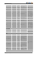
71
TXD
72#
DTR
73
PCM_OUT
74
PCM_IN
75
PCM_SYNC
76
PCM_CLK
77
GND
78
GND
79
RESERVED
80
GND
81
GND
82
MAIN_ANT
83
COEX1
84
COEX2#
85
BOOT_CFG0
86
COEX3
87
BOOT_CFG1
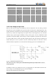
Table 3-3 Pin Function Description
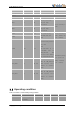
Power interface
Pin Name
Pin No.
I/O
Description
Content
VBAT
38,39,62,63
PI
Power supply voltage,
VBAT=3.4V~4.2V.
The power supply
for system Maximum
load current must
above 2A.
VDD_1V8
15
PO
Module LDO output
power ,1.8V output,Max
current 150mA,ForI/O,
MCP, WLAN/BT, SLIC,
sensors.
If not use keep it
open.
VDD_EXT
44
PO
Module LDO output
power,2.85V
output,Max current
300mA.
Only use for
external SD Card
VDD. If not use
keep it open.
GND
1,2,5,10,14,37
,40,41,43,57,5
8,60,61,64,65,
77,78,80,81
Ground.
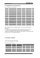
System Control
Pin Name
Pin No.
I/O
Description
Content
PWRKEY
3
DI
System power on/off
input, activelow.
RESET
4
DI
System reset input,
active low.
FLIGHTMODE
54
DI,PU
The input signal, used
to control the system
into flight mode, H:
Pull UP to
VDD_1V8(PIN 15)
with 10K resistor