
Specifications
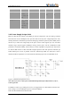

L506 Hardware Design
Copyright© Shanghai Mobiletek Communication Ltd 25
open.
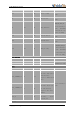
CTS
67
DO
Clear to Send.
If not use keep it
open.
RX
68
DI
Receive Data.
If not use keep it
open.
RI
69#
DO
Ring Indicator.
Multiplexed as
MDM_DBG_UART_TX.
If not use keep it
open. Recommend
reserved the test
point for debug
DCD
70
DO
Carrier detects.
If not use keep it
open
TXD
71
DO
Transmit Data.
If not use keep it
open.
DTR
72#
DI
DTE get ready.
Multiplexed as
MDM_DBG_UART_RX.
If not use keep it
open. Recommend
reserved the test
point for debug
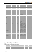
I2C interface
Pin Name
Pin No.
I/O
Description
Content
I2C_SCL
55
DO
I2C clock output.
L506 internal have
pulled up to 1.8V
I2C_SDA
56
I/O
I2C data input/output.
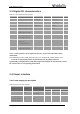
GPIO
Pin Name
Pin No.
I/O
Description
Content
GPIO_2/WAKEUP_IN
50
I/O
Default: GPIO
Optional: Input pin as
wake/interrupt
signal to module from
host.
If not use keep it
open.
GPIO_1/WAKEUP_OU
T
52
DO
Default: GPIO
Optional: Output pin
as wake/interrupt
signal to host from
module.
GPIO_0
45
DO
Default: GPIO
Optional: output
control pin.
RF port