
Specifications
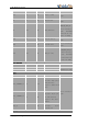

L506 Hardware Design
Copyright© Shanghai Mobiletek Communication Ltd 28
44
VCC_EXT
Power supply for
external SD card
-
2.85
-
20
USIM_VDD
Power supply for
VDD SIM
-
1.8/2.85
-
15
VDD_1V8
LDO 1.8V output
-
1.8
-
88-99*
GND
Thermal and
welding fixed
plate
-
-
-
Note: Pin88~Pin99 (total12pin) is design for the thermal welding fixed plate.
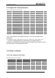
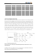
3.4.2 Power supply requirements
There are four VBAT PIN power for the module, VBAT directly power supply for the module
baseband and PA, and operating rating is 3.4V~4.2V; In the weak network environment, the antenna
will be maximum power emission. The peak current of the module under the 2G mode may reach the
peak current of 1.8A. power supply to reach 2A, the average current to reach 0.9A above. Due to the
launch of GSM/GPRS time slot pulse can cause VBAT power source instantaneous voltage drop,
maximum peak current can reach 2A, So the max power supply current must more than 2 A. Figure
3-2 sign for GSM/GPRS instantaneous pulse diagram.
Figure 3-2 GSM/GPRS instantaneous pulse
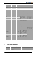
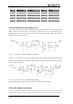
Table 3-7 VBAT power supply interface characteristics
Symbol
Description
Min
Typ
Max
Unit
VBAT
Power supply
voltage
3.4
3.8
4.2
V
IVBAT(peak)
Power supply p
current
-
2*
-
A
IVBAT(average)
Power supply
average
1
1.5
-
A