
Specifications

L506 Hardware Design
Copyright© Shanghai Mobiletek Communication Ltd 48
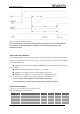
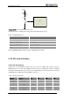
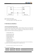
Figure 3-25boot configuration and force USB download recommended circuit
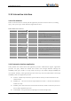
3.14 Analog and Digital conversion (ADC) interface
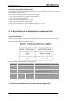
L506 integrated two analog-to-digital conversion interface, specific parameters are as follows:
Table 3-24 ADC1, ADC2 characters
characters
Min.
Typ.
Max.
Unit
ADCresolution
--
15
--
Bits
Transfer time
--
442
--
ms
Input voltage range
0.1
--
1.7
V
Input resistance
1
--
--
MΩ
Note: 1. use "AT + CADC" and "AT + CADC2" can read ADC1 and ADC2 voltage on the pin.
More information please refer to the document [1].
2. The need for special software version to support access to the ADC.
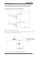
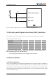
3.15 I2C interface
3.15.1 I2C pin definition
I2C is used to communicate with peripheral equipment and can be operated as either a transmitter or
receiver, depending on the device function. Both SDA and SCL are bidirectional lines connected with
I2C interface. Its operation voltage is 1.8V. High speed mode transmission rate can reach 400 KBPS,
Because L506 have internal pulled up to the I2C interface, so in your design needn’t pull up. Figure
3-26 is the reference design:
L506
1.8V
BOOT_CFG0
10K
BOOT_CFG0
COEX2/FORCE_USB_BOOT
SW3
SW1
SW2