
Specifications

L506 Hardware Design
Copyright© Shanghai Mobiletek Communication Ltd 51
4 Product characteristics
4.1 Absolute parameters
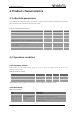
The following table shows the state of the absolute maximum work in abnormal situation.Exceed the limit
value will likely result in permanent damage to the module.
Table 4-1L506 absolute parameters
Parameter
Min.
Max.
Unit
VBAT absolute voltage parameter
-0.5
6.0
V
USB_VBUSabsolute voltage parameter
-0.5
5.25
V
I/O absolute voltage parameter:
PWRKEY,RESET,SPI,GPIO,I2C,PCM,UART,SD1_DET,USIM_DET
-0.3
2.1
V
I/O absolute voltage parameter:
SD and USIM
-0.3
3.05
V
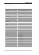
4.2 Operation condition
4.2.1 Operation voltage
This product is a DC input voltage range of 3.4 V to 4.2 V, the typical value of 3.8 V, as s
hown in below table.
Table 4-2 Input DC voltage
Parameter
Min.
Typ.
Max.
Unit
VBAT Voltage
3.4
3.8
4.2
V
USB_VBUS Votage
2.0
5.0
5.25
V
About L506 dc electric property, please refer to part 3.3 digital I/O characteristics.
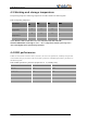
4.2.2 Work mode
Table 4-3 work mode
Mode
Description
Normal operation
mode
(GSM/WCDMA
/TD-SCDMA/EVDO/LTE)
Sleep
In this case, the current consumption of module
will bereduced to the minimal level.
In sleep mode, the module can still receive paging
message and SMS.