
Specifications

L506 Hardware Design
Copyright© Shanghai Mobiletek Communication Ltd 56
body to produce attenuation; But also to reduce the radiation and the structure of the realization of the
need to take into account. So, At the beginning of the design need to structure, ID, circuit, antenna
engineers together to evaluate the layout.
Antenna matching circuit
If the module's radio frequency port and the antenna interface need to be transferred, the main board
circuit design, The design of microstrip line or strip line between the module RF test base and the
antenna interface between the microstrip line or the strip line by characteristic impedance 50 ohm, at
the same time, reserved double L type matching circuit; If the antenna's RF connector can be directly
stuck in the module's RF test base, can save the module of the RF port and the antenna interface
between the transfer.
5.4 EMC and ESD design advice
Users should take full account of the EMC problem caused by signal integrity and power integrity in
the design of the whole machine, In the module of the peripheral circuit layout, for power and signal
lines, etc., to maintain the spacing of 2 times line width. Can effectively reduce the coupling between
the signal, so that the signal has a clean, the return path. When the peripheral power supply circuit is
designed, the decoupling capacitor should be placed close to the module power supply pin, High
frequency high speed circuit and sensitive circuit should be far from the edge of PCB, and the layout
of the layout as far as possible to reduce the interference between each other, and the sensitive signal is
protected. The circuit or device that may interfere with the operation of the system board is designed.
This product is embedded in the system board side, design, need to pay attention to the ESD protection,
the key input and output signal interface, such as (U) SIM card interface need to be placed close to the
protection of ESD devices. In addition to the motherboard side, the user is required to design the
structure and PCB layout, ensure that the metal shield is fully grounded, and set up an unobstructed
discharge passage for the electrostatic discharge.
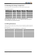
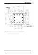
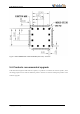
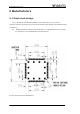
5.5 PCB Recommended land pattern
We recommend that users in the design of main board PCB DEF,In the middle of the 12 geothermal
solder design according to size in below figure. Recommended at 87 of peripheral signal pads to the
module with a length of 1.0 mm.Recommended PCB pads as shown in below.