
Data Sheet

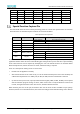
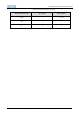


Table Of Contents
- Abstract
- 1. Introduction
- 2. Characteristics
- 3. Pin Definition
- 4. System memory Space
- 5. ATE(RF Test Mode)
- 5.1. Wi-Fi ATE Command
- 5.1.1. Start MP mode
- 5.1.2. Stop MP mode
- 5.1.3. Set Tx rate
- 5.1.4. Set operational channel
- 5.1.5. Set operational bandwidth
- 5.1.6. Set Tx power
- 5.1.7. Set antenna for Tx
- 5.1.8. Set antenna for Rx
- 5.1.9. Start air Rx mode
- 5.1.10. Start continuous Tx mode
- 5.1.11. Query air Rx statistics
- 5.1.12. Reset air Tx/Rx statistics
- 5.2. Bluetooth ATE Command(TBD)
- 5.3. Example Command
- 5.1. Wi-Fi ATE Command
- 6. Flash Programming
- 7. Electrical Parameters
- 8. RF Parameter
- 9. Antenna Information
- 10. Dimensions and Production Guidance
- 11. Production Guidelines
- 12. FCC and IC Information
- 12.1. FCC Warning
- 12.2. IC warning
- 12.3. Trace antenna designs
- 12.4. RF exposure considerations
- 12.5. Antennas
- 12.6. Label and compliance information
- 12.7. Information on test modes and additional testing requirements5
- 12.8. Additional testing, Part 15 Subpart B disclaimer
- 12.9. The module is limited to OEM installation ONLY.
- 12.10. The OEM integrator is responsible for ensuring that the end-user has no manual instructions to remove or install module.
- 12.11. The module is limited to installation in mobile or fixed applications
- 13. Packaging and Label Information
- 14. Sales and Technical Support Information

EMC3380 Series Wireless Module Data Manual
Copyright of Shanghai MXCHIP Information Technology Co., Ltd.
21
SPI Flash Memory
The CPU manages access to flash memory from the I-Code and D-Code buses via the built-in SPI
Flash Control Unit (SPIC). At the same time, operations such as erasure, programming, and read-write
protection are also implemented, and the execution of code stored in flash memory is accelerated by
instruction prefetch and cache.
PSRAM
4M bytes PSRAM, using 50MHz DDR memory.
System storage control address allocation
Address allocation is as following table.
Table 6 System storage space
Base Address
Top Address
Size
Function
Description
0x0000_0000
0x0001_FFFF
128KB
KM0 ITCM ROM
(actually 96KB)
32MB: KM0 Memory
Address
0x0002_0000
0x0002_7FFF
32KB
KM0 DTCM ROM
(actually 16KB)
0x0002_8000
0x0007_FFFF
352KB
RSVD
0x0008_0000
0x0008_FFFF
64KB
KM0 SRAM
0x0009_0000
0x000B_FFFF
192KB
RSVD
0x000C_0000
0x000C_3FFF
16KB
Retention SRAM
(1KB) (the same
port with KM0
SRAM)
0x000C_4000
0x000F_FFFF
240KB
RSVD
0x0010_0000
0x01FF_FFFF
31MB
RSVD
0x0200_0000
0x07FF_FFFF
96MB
PSRAM
224MB: External
Memory
Address
0x0800_0000
0x0FFF_FFFF
128MB
External FLASH
0x1000_0000
0x1007_FFFF
512KB
KM4 SRAM
256MB: KM4
Memory
Address
0x1008_0000
0x100D_FFFF
384KB
RSVD
0x100E_0000
0x100E_FFFF
64KB
Extension SRAM0
from Bluetooth
0x100F_0000
0x100F_FFFF
64KB
Extension SRAM1
from Wi-Fi
0x1010_0000
0x1013_FFFF
256KB
KM4 ITCM ROM
0x101C_0000
0x101D_7FFF
96KB
KM4 DTCM ROM
0x101E_0000
0x101F_FFFF
256KB
RSVD
0x1020_0000
0x1FFF_FFFF
254MB
RSVD
0x2000_0000
0x3FFF_FFFF
512MB
RSVD
Reserved