
Data Sheet
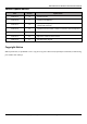

Table Of Contents
- Abstract
- 1. Introduction
- 2. Characteristics
- 3. Pin Definition
- 4. System memory Space
- 5. ATE(RF Test Mode)
- 5.1. Wi-Fi ATE Command
- 5.1.1. Start MP mode
- 5.1.2. Stop MP mode
- 5.1.3. Set Tx rate
- 5.1.4. Set operational channel
- 5.1.5. Set operational bandwidth
- 5.1.6. Set Tx power
- 5.1.7. Set antenna for Tx
- 5.1.8. Set antenna for Rx
- 5.1.9. Start air Rx mode
- 5.1.10. Start continuous Tx mode
- 5.1.11. Query air Rx statistics
- 5.1.12. Reset air Tx/Rx statistics
- 5.2. Bluetooth ATE Command(TBD)
- 5.3. Example Command
- 5.1. Wi-Fi ATE Command
- 6. Flash Programming
- 7. Electrical Parameters
- 8. RF Parameter
- 9. Antenna Information
- 10. Dimensions and Production Guidance
- 11. Production Guidelines
- 12. FCC and IC Information
- 12.1. FCC Warning
- 12.2. IC warning
- 12.3. Trace antenna designs
- 12.4. RF exposure considerations
- 12.5. Antennas
- 12.6. Label and compliance information
- 12.7. Information on test modes and additional testing requirements5
- 12.8. Additional testing, Part 15 Subpart B disclaimer
- 12.9. The module is limited to OEM installation ONLY.
- 12.10. The OEM integrator is responsible for ensuring that the end-user has no manual instructions to remove or install module.
- 12.11. The module is limited to installation in mobile or fixed applications
- 13. Packaging and Label Information
- 14. Sales and Technical Support Information

EMC3380 Series Wireless Module Data Manual
Copyright of Shanghai MXCHIP Information Technology Co., Ltd.
4
Sales and Technical Support Information ............................................................................................. 55
Table Catalog
Table 1 EMC3380 peripheral list ......................................................................................................................... 7
Table 2 EMC3380 Pin Definition ...................................................................................................................... 14
Table 3 Low energy pin definition ..................................................................................................................... 17
Table 4 Special Function Capture Pin ................................................................................................................ 18
Table 5 Firmware special function capture pin .................................................................................................. 19
Table 6 System storage space ............................................................................................................................ 21
Table 7 MXOS 4M byte Flash storage space partition ...................................................................................... 22
Table 8 Flash programming methods ................................................................................................................. 28
Table 9 Input Voltage Range .............................................................................................................................. 32
Table 10 Absolute maximum parameter: voltage .............................................................................................. 32
Table 11 operating parameter: voltage and current ............................................................................................ 32
Table 12 Average power consumption under 3.3V ............................................................................................ 32
Table 13 RF consumption under 3.3V ............................................................................................................... 34
Table 14 operation parameter(3.3V):Digital IO DC characteristic ............................................................... 34
Table 15 RF Standard ........................................................................................................................................ 35
Table 16 EMC3380 IEEE 802.11b TX/RX Characteristics Parameters ............................................................ 35
Table 17 EMC3380 IEEE802.11g module TX/RX Characteristics Parameters ................................................ 36
Table 18 EMC3380 IEEE802.11n-HT20 RX/TX Characteristics Parameters ................................................... 37
Table 19 EMC3380 IEEE802.11n-HT40 RX/TX Characteristics Parameters ................................................... 37
Table 20 EMC3380 IEEE802.11a RX/TX Characteristics Parameters ............................................................. 38
Table 21 EMC3380 IEEE802.11n-HT20(5G RX/TX Characteristics Parameters ............................................ 39
Table 22 EMC3380 IEEE802.11n-HT40(5G) RX/TX Characteristics Parameters ........................................... 40
Table 23 EMC3380 BLE4.0 TX/RX RX/TX Characteristics Parameters ......................................................... 41
Table 24 EMC3380 BLE5.0 TX/RX RX/TX Characteristics Parameters ......................................................... 42
Table 25 Module MOQ and Packaging Information ......................................................................................... 54
Figure Catalog
Figure 1 EMC3380 Hardware Block Diagram .................................................................................................... 6
Figure 2 EMC3380 Pin Arrangement ................................................................................................................ 13
Figure 3 Audio noise reduction chip BR262 connection schematic diagram .................................................... 17
Figure 4 The Schematic Diagram of ATE Mode Connection ............................................................................ 23